
I liked the Genos block diagrams which I posted the other day. The diagrams summarize the Genos main CPU and tone generation subsystems in a compact form.
So, let’s move on to Montage. The diagrams below are taken from the Yamaha Montage Service Manual. I scrubbed non-essential detail (e.g., power rails) in order to focus on the overall digital system organization.
The internal design of mid- and high-end synths and arrangers separates neatly into a main CPU subsystem (running Linux) and a tone generation/digital audio subsystem. Genos, Montage and MODX fit this design pattern.
[Click images to enlarge.]
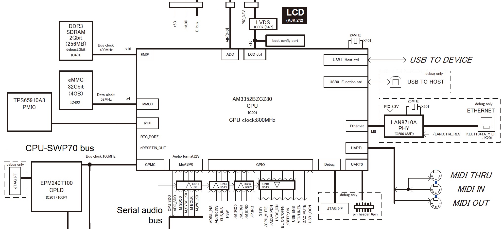
The Montage main CPU is a Texas Instruments AM3352. Montage has a slightly lower clock rate: 800MHz vs. 1.0GHz (Genos). I don’t think the difference in clock speed is significant because the main CPU generally doesn’t perform compute intensive tasks. (The tone generator circuits and the audio DSP do the heavy lifting.) The main CPU handles sequencing, user interface, the file system, etc.
The AM3352 is an ARM Sitara Cortex-A8 32-bit “system on a chip.” The AM3352 is designed for embedded applications and as such, it has many integrated input/output (I/O) interfaces. The main interfaces are:
- Primary working memory (EMIF)
- Touch panel and display (LCD)
- Bulk memory (MMC0)
- USB to device interface (USB1)
- MIDI I/O (UART1)
- Serial digital audio bus (McASP0)
- CPU-SWP70 bus (GPMC)
- Power management (I2C0)
- General purpose I/O (GPIO)
Having so many interfaces in one integrated circuit (IC) package lowers cost signficantly.
Memory resources are modest. Primary memory is only 256MBytes. Bulk storage is provided by a 4GByte eMMC embedded memory device. Linux and user data (performances, songs, arpeggios, etc.) reside in the eMMC device. Please note that the bulk memory bus (MMC0) has a relatively slow clock speed (52MHz) and width (4 bits). Simply put, this bus cannot support real-time sample streaming for synthesis. [Please stop ranting about this on the Web.] Instead, waveform samples are stored in NAND flash connected to the Master SWP70 tone generator.
Speaking of tone generation, the main CPU is connected to two SWP70 tone generation ICs by the CPU-SWP70 bus. The bus is mediated by a programmable logic device (CPLD). The bus clock is 100MHz. The bus has 19 address bits and the data path is 16 bits wide. The CPU sends control data to the SWP70s through this bus. Also, the main CPU loads samples into NAND flash using this bus. I doubt if this bus could sustain high volume sample streaming in real time.
The CPU-SWP70 bus is organized as an addressable memory bus. (The ARM acronym “GPMC” means “General Purpose Memory Controller.”) Instead of ordinary memory, I believe that the CPU-SWP70 bus provides direct access to thousands of synthesis control registers for AWM2 and FM-X. Check out the huge list of synthesis parameters in the MIDI section of the Montage/MODX Data List PDF. Each parameter controls some aspect of AWM2 or FM-X synthesis. These parameters need to be loaded quickly into the the SWP70 tone generation blocks. Addressable control registers provide the appropriate mechanism.
There are two other major busses in Montage: the EBUS and the serial digital audio bus. (More about the digital audio bus in a second.) The EBUS is driven by an ARM architecture microcontroller (MB9AF141NBPQC) which scans knobs, sliders and switches. The EBUS sends user input to other components, most notably the SWP70s. Thanks to the EBUS, user inputs are quickly acquired and sent to the tone generation process, thereby minimizing latency. This fast path is an important aspect of Yamaha’s design.
On to tone generation and digital audio!
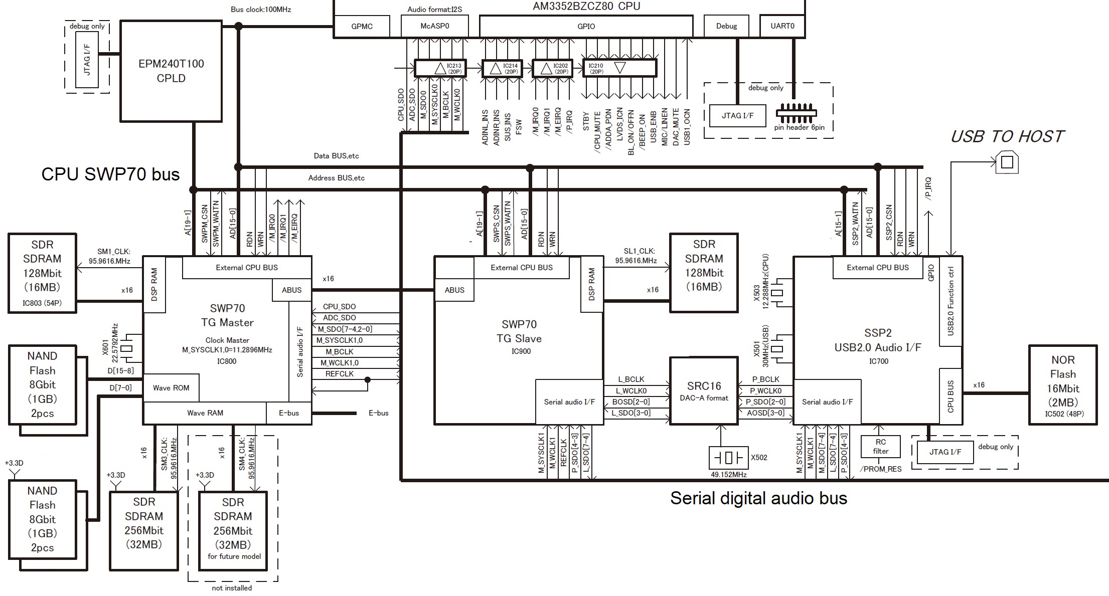
High-end Yamaha synths and arrangers have two SWP70 (“Standard Wave Processor”) tone generation chips. One SWP70 is the Master and the other SWP70 is the Slave. “Master” and “Slave” refer to the communication relationship between the two components. The Master generates the reference clocks for both the Master and Slave, and it generates the clock for the serial audio bus.
In Montage, the Master SWP70 performs AWM2 synthesis and the Slave performs FM-X synthesis. The Master has waveform memory; the Slave does not. Waveform memory isn’t required for FM-X synthesis, apparently.
Both the Master and Slave SWP70s have 16MBytes of DSP RAM apiece. The DSP RAM provides big, fast random access storage for effects processing. Time-based effect algorithms like reverb and delay need a large amount of memory space. The DSP RAM does the job.
The Master SWP70 has two additional kinds of memory: Wave ROM (4GBytes physical capacity) and Wave RAM (32MBytes). [The Genos designers use slightly different terminology for these units, but the functionality is the same.)
Wave ROM is Open NAND Flash Interface (ONFI) compliant. This is the same commodity NAND flash built into PC solid state drives. Instead of using a solid state drive and a SATA bus, Yamaha have built the controller and data cache into the SWP70. This design eliminates the cost, power consumption and delay of a PC solid state drive controller. The Wave RAM is the data cache, holding the currently used samples needed for AWM2 synthesis.
Why a data cache? NAND flash has two major drawbacks. First, writing to NAND flash is slow. Second, random read access to NAND flash is much slower than sequential block access. In fact, random access is too slow for direct streaming into synthesis. The SWP70 pre-fetches blocks of samples into fast Wave RAM which, in turn, provides fast random access to samples. This two-level storage organization supports the high read bandwidth required for 128 lanes of stereo AWM2 synthesis.
The SWP70 has two independent Wave RAM channels. Only one of these channels is populated in Montage. The second Wave RAM unit is not installed and is reserved for a future model. We haven’t seen the full power of the SWP70 generation — yet.
Montage has a power digital audio subsystem which is interconnected by the serial digital audio bus. The CPU, SWP70s and SSP2 chips transfer digital audio on the serial audio bus. These units send audio to the digital-to-analog converters (DACs) and receive audio from the analog-to-digital converters over the bus. The main audio streams are:
- The main CPU receives audio from the AD INPUT ADC and the Master SWP70.
- The Master SWP70 receives audio from the main CPU and the AD INPUT ADC.
- The Slave SWP70 receives audio from the SSP2.
- The SSP2 receives audio from the Master SWP70 and the Slave SWP70.
The Master SWP70 sends digital audio to the two DACs (assignable output and main output, respectively). The DACs and the ADCs are on a separate circuit board away from the digital electronics (Pure Analog Circuit).
Montage has an SSP2 processor dedicated to USB2.0 audio I/O. It’s like having a mini Steinberg UR interface inside. The SSP2 is the source of Montage’s audio prowess. The SSP2 is a fairly beefy computational engine having an SH-2 CPU core (135.4752MHz internal clock). It is the computational engine in the high-end Steinberg UR series, the Reface DX and the Reface CS. Its role in Montage is like a UR — high speed, multi-channel USB audio. This is why the SSP2 supplies the Montage USB TO HOST interface. Digital USB audio has a direct path to the USB HOST.
The SSP2 gets commands and transfers data with the main CPU over the CPU-SWP70 bus.
I hope you have found this quick tour to be informative and helpful. Yamaha had a few other tricks up its sleeve as we shall see when I discuss MODX specifically. Take care and stay tuned for the MODX update which is about to drop.
Copyright © 2019 Paul J. Drongowski
Diagrams are Copyright Yamaha