
Folks are speculating about the wave memory in the new Yamaha Montage. Without the actual service manual in hand, it’s impossible to be definitive. However, I think it’s reasonable to assume that:
- The Montage uses the new SWP70 tone generator, and
- The wave memory interface is the same as the PSR-S970.
Here’s a few details about the SWP70 and wave memory interface in the PSR-S970 arranger workstation. If you buy into the two assumptions above, then these details should apply to the Montage as well.
I realize that my earlier posts dive deep and cover many aspects of the SWP70. This blog post concentrates on a few specific aspects of the wave memory interface in the PSR-S970 instead of the whole she-bang.
The SWP70 has two 8-bit memory data ports — HIGH and LOW — and a common set of wave memory control signals. The interfacing standard is the Open NAND FLASH interface (ONFI). One flash memory device plugs into the HIGH port and a second flash memory device plugs into the LOW port. The two flash memory devices share the control signals, that is, the same control signals are routed to both memory devices.
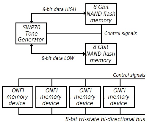
The PSR-S970 memory devices are Spansion S34ML08G1 8Gbit NAND flash memory devices. The S34ML08G1 is a dual-die stack of two S34ML04G1 die. Spansion currently produces the S34ML16G2, which is a quad-die stack of four S34ML04G1 die.
Thanks to ONFI, the 16Gbit (2 GByte) S34ML08G1 is pin compatible with the smaller S34ML08G1. Thus, a tone generator complex with twice the wave memory capacity can be built in the same printed circuit board (PCB) footprint.
The ONFI bus is not the same as the old flash expansion memory DIMM interface as provided in the later Tyros and Motif/MOXF products. The DIMM expansion memory interface consists of two, full-parallel memory channels with separate address and data signals for each channel. An ONFI memory device, on the other hand, has a single bi-driectional (tri-state) data port. The memory address, data and control information are sent to the memory device in byte-serial fashion. (The bus is time-division multiplexed.)
The tri-state electrical interface supports expansion by plugging multiple memory devices onto the same 8-bit multiplexed bus. The control signals and protocol choose the device that drives (or reads) the tri-state bus at a given time.
Yamaha may not have found a convenient way to make the ONFI bus user-extensible. Or, Yamaha have simply decided to not provide end-user wave memory expansion in the field. Yamaha accrue several benefits by dropping the DIMM expansion slots:
- The cost of the DIMM connector(s) is eliminated including the cost of mounting and testing the connectors.
- PCB size is greatly reduced.
- The access cover and chassis hole are eliminated.
- The cost of stocking another part/SKU is eliminated.
The disadvantage to the end-user is “All the sample space you get is built-in right from the start and no more.”
Yamaha’s new approach to user waveform memory is to reserve space for user samples in the physical wave memory. In other words, the user expansion memory is contained in the same physical package (48-Pin TSOP 12mm x 20mm x 1.2 mm) as the factory waveforms. The Montage specifications describe wave memory as:
Preset: 5.67 GB (when converted to 16 bit linear format), User: 1.75 GB
The compressed factory waveforms occupy 2.835 GBytes of physical memory (assuming a 2-to-1 compression factor). Compressed user waveforms require 0.875 GBytes of physical memory. These figures point toward a 4 GByte physical wave memory size, which would reserve some space for Yamaha’s own future use. BTW, if the actual effective compression factor is higher, then user samples could be stored uncompressed.
For reference, here is a terse summary of the Spansion S34ML08G1 device that is used in the PSR-S970:
    Spansion S34ML08G101TFI000
    Density: 8Gbits (4Gbits x 2)
    Random access: 30us (max)
    Sequential access: 25ns (Min)
    Block erase time: 3.5ms
    Program time: 300 us (typical)
    Data retention: 10 years (typical)
    100,000 program/erase cycles (typical)
    Pricing: $7.84 USD (quantity 250 up)
The data retention time (10 years) should raise a few eyebrows. NAND flash is volatile and charge (data) is eventually lost unless it is refreshed. I wonder how many manufacturers have planned for the day when keyboards, phones or whatever lose presumably “permanent” data stored in flash? Mask-programmable ROM never had this problem… I don’t think Hank done it this way.
Update: Read more about NAND flash data retention.
All site content Copyright © Paul J. Drongowski unless otherwise indicated