Yamaha Genos: Tone generation

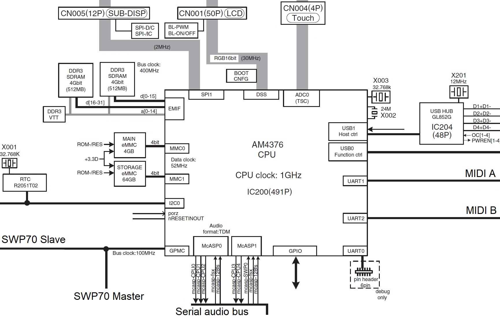
After visiting the Genos CPU complex yesterday, let’s take a look at the two Yamaha SWP70 tone generators in Genos.

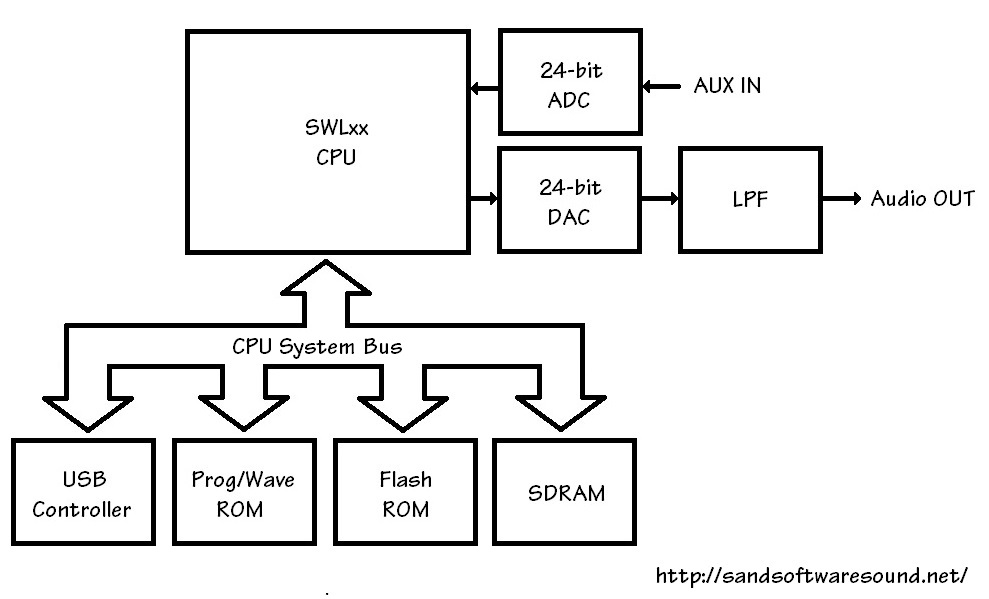
The SWP70 is the latest generation, top-of-the-line Yamaha tone generator. We know that the SWP70 is capable of both sample-playback AWM2 synthesis and FM-X synthesis as demonstrated by the Yamaha Montage and MODX.

[Click image to enlarge.]

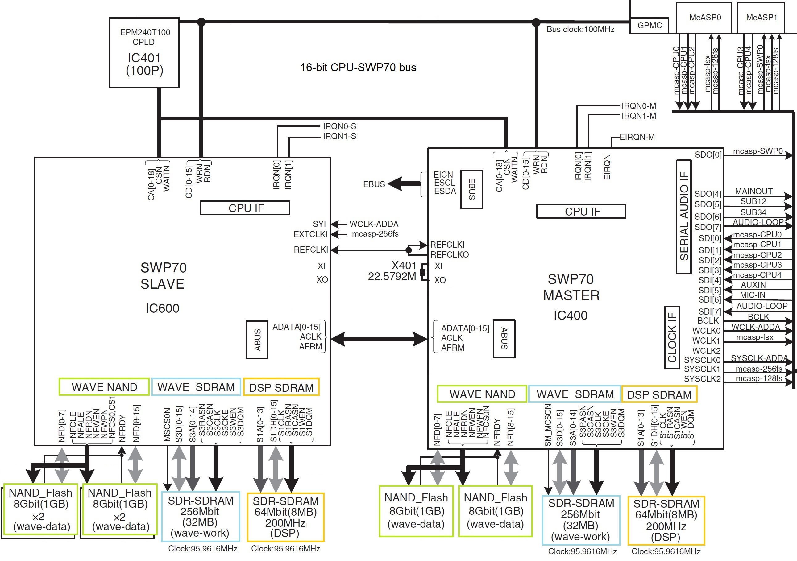
The two SWP70s are organized as a master and slave pair, each with different connections and dedicated memory units. The SWP70s communicate with the TI AM4376 processor over the CPU-SWP70 bus. The bus is arbitrated by a programmable logic device (CPLD). The data path is 16 bits and there are 19 address bits. Bus clock speed is 100MHz.

The main CPU sends control messages, etc. to the SWP70s through this bus. The main CPU also uses this bus to write waveforms (“samples”) in the SWP70 wave memory. Please note that the 100MHz bus isn’t fast enough to sustain so-called sample streaming from bulk storage. As mentioned in my previous article about the main CPU, the embedded bulk memory devices (eMMC) would not be able to supply samples fast enough for streaming either. Plus, write time to NAND flash is quite slow — another strike against streaming.

The Master SWP70 has extensive connections to the serial digital audio bus that interconnects the main CPU, tone generation, analog to digital converstion (ADC) and digital to analog conversion (DAC). Here’s a few notable connections:

  • The main CPU sends five digital audio streams to the Master SWP70.
  • The Master SWP70 sends one digital audio stream to the main CPU.
  • The Master SWP70 sends the MAIN OUT, SUB 12 and SUB34 streams to their respective DACs.
  • The Master SWP70 receives the AUX IN and MIC IN streams from their respective ADCs.
  • The AUDIO-LOOP stream is a loop-back from the Master SWP70 to the Master SWP70.

Genos serial digital audio resources and capabilities are substantially less than Montage. In short, Montage has a Yamaha SSP2 processor dedicated to digital audio much like a Steinberg UR interface. This version of the Genos hardware will never have the extensive digital audio capabilities of Montage.

Another important interface is the Yamaha EBUS. Genos has an ARM M3 microcontrollers that scan the knobs, sliders, buttons and keys. The microcontroller sends these inputs on the EBUS. The EBUS is a slow-speed, serial I2C bus. User inputs are quickly encoded and are sent directly to tone generation. Nifty. The direct connection decreases latency by keeping the main CPU out of the message path. Montage and MODX have an EBUS, too. It’s an essential feature of Yamaha high-end design.

As Gandolf would say, “On to the Forest of Memories!”

Each SWP70 has two working memories:

  • WAVE SDRAM (light blue)
  • DSP SDRAM (orange)

Both working memories have dedicated address and data paths. The data paths are sixteen bits wide. The required memory capacity is too large to integrate on the SWP70 integrated circuit (IC), so separate commodity memory devices are used instead.

The DSP SDRAM is working memory for DSP computations. Certain kinds of effects are memory intensive — reverb and delay effects, in particular. The DSP SDRAM is a fast read/write working memory for effects processing.

The WAVE SDRAM is the working memory which holds the most recently streamed and used waveform samples. Random access to data in NAND flash is relatively slow. The WAVE SDRAM is a fast random access cache for samples in current use. The SWP70 behaves like the controller and cache within a commodity solid state drive. It streams waveform samples into cache as fast as possible via sequential reads to the WAVE NAND. The incoming samples are stored in the WAVE SDRAM and are played back from WAVE SDRAM.

Yamaha’s architecture is often (unfairly) slagged on two points:

  • Why doesn’t Yamaha stream from a commodity SSD?
  • Why doesn’t Yamaha use a commodity x86 motherboard for tone generation?

Yamaha combined the best parts of a commodity SSD and hardware tone generation in one component (the SWP70). This is a strategic low-latency advantage. The SSD SATA bus is quite unnecessary. The Yamaha architecture lowers power consumption, component count and most importantly, latency.

As to commodity motherboard, see Korg Kronos (big, heavy and hot).

WAVE NAND memory (light green) is implemented using commodity Open NAND Flash Interface (ONFI) devices. This is the same NAND flash employed in commodity, SATA-based SSDs. The Slave SWP70 has four gigabytes (4GBytes) of waveform memory while the Master SWP70 has two gigabytes (2GBytes). Storage is split into upper and lower bytes for a total data path width of 16 bits. The SWP70 accesses the upper and lower bytes in parallel. (Each ONFI channel is 8 bits wide.) Thus, Yamaha double the transfer bandwidth from NAND flash.

Presumably, the Slave WAVE NAND contains the Genos factory preset waveforms and the Master WAVE NAND contains user expansion waveforms. The Genos specifications split polyphony between preset and user voices. Expansion memory is limited to something just shy of 2GBytes. So, this inference is reasonable.

Now that you’ve read this far, you should have solid footing in Yamaha synth and arranger hardware architecture. Of course, there are many additional details about clock speeds, displays, touch panel, etc. However, you should have a better appreciation for and understanding of the basic data flows and storage units.

Copyright © 2019 Paul J. Drongowski

Source: Yamaha Genos Service Manual (Copyright Yamaha)

[Update: 18 October 2019]

Just a quick addendum about the SSP2 chip and the Steinberg URs. The SSP2 is built into the UR242, UR44, UR28M and UR824. Steinberg have a spiffy iOS app, dspMixFx, which exposes the SSP2’s functionality. Quoting Steinberg:

dspMixFx brings the flexibility and sound of Yamaha’s SSP2 DSP chip to your iOS device. Built in Steinberg’s UR824, UR28M, UR44 and UR242 interfaces, this custom-designed DSP chip runs the acclaimed REV-X reverb, Sweet Spot Morphing Channel Strip and Guitar Amp Classics effects. The free dspMixFx app allows you to control all DSP features and create your own latency-free mixes on your iPad and iPhone with effects, ideal for live recording sessions where getting exactly the right sound for performers is paramount. dspMixFx is also compatible with other iOS audio apps, offering full operation when using third-party apps with the DSP-powered interfaces in Steinberg’s UR range.

The REV-X reverb built into the UR824, UR28M, UR44 and UR242 is a complex reverb algorithm developed by Yamaha. Renowned for its high density, richly reverberant sound quality, with smooth attenuation, spread and depth that work together to enhance the original sound, the REV-X features three types of reverb effects: Hall, Room and Plate simulations with reverb time and level control.

Thanks to its SSP2 chip, the Montage provides conversion to and from a DAW roughly on par with a Steinberg UR interface.

Yamaha Genos: Main CPU

After a long move and a hiatus from writing, it’s time to dig into digital design.

I get a little anxious when I see people speculating about the internal operation of synthesizers and arrangers. They often assume that:

  • A keyboard instrument is organized just like a PC.
  • Samples are streamed from some kind of magnetic or solid-state disk.
  • The main CPU runs the tone generation software.
  • Samples are held in the main CPU’s memory during tone generation.

These assumptions are not true for Yamaha Genos, Montage or MODX.

These musical instruments are organized internally like an embedded hardware device. Sure, there is a main computer inside, but it is an embedded processor with many input/output (I/O) interfaces integrated onto the same integrated circuit (IC). This kind of organization is often called an “SOC,” or “System on a chip.”

[Click on image to enlarge.]

The diagram (above) shows the main CPU in Yamaha Genos. It is a Texas Instruments AM4376 embedded ARM processor. You can see that it has many integrated I/O ports: two USB ports, three serial interface ports (UART), parallel digital pins (GPIO), serial audio (McASP), real-time clock (RTC), and display and touch panel ports. Of course, there are also RAM (EMIF) and bulk storage (MMC) interfaces, too. Finally, there is a 16-bit bus connecting the main CPU to the two Yamaha SWP70 tone generator chips.

Before moving into important details, here’s a few quick observations:

  • The USB1 port connects to an internal 4-port USB hub. The hub provides external interfaces: TO DEVICE (front), TO DEVICE (bottom), USB TO DEVICE, and an internal wireless LAN module (UD-WL01).
  • The USB0 port provides the external USB TO HOST interface.
  • UART1 provides the 5-pin MIDI A data signals and and UART2 provides the 5-pin MIDI B data signals.
  • Digital audio is transferred on an internal serial audio bus using time division multiplexing (TDM). Serial digital audio is 2 channel, 24-bit I2S compatible, allowing direct communication with the audio converters (ADCs and DACs)

Montage has a more extensive digital audio subsystem — one of the reasons why Montage supports studio-level audio conversion.

RAM capacity is modest: 512MBytes. The Linux operating system and Genos control software reside in this memory during operation. Suffice it to say, this is no where near enough to store samples for tone generation. Tone generation is handled by the SWP70 integrated circuits.

There are two embedded bulk storage memories: 4GBytes and 64GBytes. Linux boots from the 4GByte device. The 64GByte device provides the user expansion memory. Please note the data clock speed (52MHz) and data bus width (4 bits), which adhere to the eMMC protocol. There is enough bandwidth to support a single digital audio stream, but not near enough bandwidth for tone generation. I might add that the 100MHz 16-bit bus to the SWP70s is not enough bandiwdth either.

I hope this short article provides a bit of insight about the modest computational and memory resources of the Genos main CPU. When I get a chance, I’ll give a short tour of Genos’s tone generation section.

Source: Yamaha Genos Service Manual (Copyright Yamaha)

Copyright © 2019 Paul J. Drongowski

All is swell (SWL)

Yamaha develop a wide range of keyboard products from low-cost entry-level ‘boards to high-end synthesizers and digital workstations (AKA “arrangers”).

Within a market segment, the engineering challenge is to develop, manufacture and test a product with the desired feature set at the target selling price. I won’t discuss profit margin here since no one really knows, but Yamaha. We do know, however, that amortized non-recurring and recurring costs must be low enough to produce a significant return. Cost sensitivity is simply a day-to-day reality.

The entry-level segment is the most cost-sensitive segment because most customers in this segment are looking for an inexpensive keyboard with basic functionality. Think “Parents buying a first keyboard for a kid who may walk away from the whole thing in a week or two.” The entry-level segment outsells the mid- and high-end portable keyboard segment by nearly 2 to 1:

    Category                       Units            Retail value
    -----------------------------  ---------------  -------------
    Acoustic guitars               1,499,000 units  $678,000,000
    Electric guitars               1,132,000 units  $506,000,000
    Digital pianos                   135,000 units  $165,000,000
    Keyboard synthesizers             81,000 units  $104,000,000
    Controller keyboards             160,000 units  $ 32,000,000
    Portable keyboards under $199    656,000 units  $ 64,000,000
    Portable keyboards over $199     350,000 units  $123,000,000
    Total portable keyboards       1,006,000 units  $187,000,000

    Sales Statistics for 2014, USA market

Synth fanatics should note that although the average selling price (ASP) is higher for synths, the portable keyboard segment moves a much higher number of units. Fortunately, for manufacturers playing in the entry-level portable keyboard space, volume is relatively high and non-recurring cost can be laid off across a larger number of units than synths.

The entry-level segment has one other important driver — the desire for portable, battery operation. This design consideration limits the amount of electrical power available for computation and thus, limits the amount of computational capacity itself. Some dynamic power can be bought back through lower CPU clock speeds. Folks accustomed to giga-Hertz CPUs may be shocked to see such low clock speeds! Lower clock speeds simplify cooling and reduce overall weight by eliminating heat sinks and cooling fans.

LSI vs. commodity

Yamaha perceive their proprietary expertise in large scale integration (LSI) as a competitive advantage. Although Yamaha exploit commodity components where possible, tone generation and digital signal processing (DSP) are performed in proprietary hardware.

User interface and control (e.g., USB communications, MIDI, LCD, etc.) are a good fit with commodity CPU technology. Yamaha — and Roland — have a long history with H8 and SH architecture CPUs from Hitachi, now Renesas. Early products employed H8 microcontrollers for host CPU functions. Yamaha eventually migrated to the “Super H” reduced instruction set computer (RISC) family. (In 2011, Renesas announced the end of the H8 line.)

Yamaha have a considerable investment in software built and tuned for the SH family. Thus, migration to a new commodity architecture (ARM) is a pretty big deal with a high internal cost. Yamaha have adopted ARM for panel scanning/control in Reface and are using ARM processors for host computation in Montage and Genos. Time and experience will show if ARM is adopted in the entry- and mid-range segments, too.

Old faithful

Yamaha’s entry-level models rely on “old faithful,” the SWL family of proprietary Yamaha processors. The SWL is used in all entry-level models — a good way to drive volume manufacturing of a custom part. The SWL family has undergone several revisions over the years. I don’t intend to recount that history here.

The SWL01U was used in many products including the PSR-E443. The external clock crystal oscillates at 16.9344MHz yielding an internal clock speed of 33.8688MHz by scaling. The relatively low clock speed reduces heat and power consumption. The following diagram shows the typical “compute complex” in an entry-level keyboard. [Click to enlarge.]

The structure in the diagram is generic across Yamaha entry-level products. If you dive into the service manual for a specific entry-level keyboard, you’re likely to find a “compute complex” like this generic one although memory capacities and such are model specific.

The SWL01U provides a CPU bus to which a USB controller (optional), program/wave ROM, flash ROM and SDRAM are attached. The SWL01 has many on-board interfaces: keyboard scanning, LED/LCD interface, bit-serial audio (ADC, DAC), control knob sensing, etc. The SWL01U has an integrated USB controller which can be deployed in ultra low-cost, minimum component count designs.

The SDRAM is, of course, read/write working memory. The flash ROM retains user data when power is turned off.

The program and waveform data are stored in the same physical memory component. In the case of the PSR-E443, the prog/wave memory is a 16MByte parallel NOR flash memory. The factory sound set, therefore, is smaller than 16MBytes. Panel voices, the XGlite sound set, and drum kits are crammed into this small memory along with the E443’s software.

The SWL01U integrates 32 tone generation channels and relatively “lite” DSP effects (reverb, chorus and flanger). I have not had the chance to browse the service manual for the PSR-E453 (or E463). E453 polyphony increased to 48 voices and the DSP effect types got a modest bump. I expect to find a new, updated member of the SWL family in these newer keyboards.

Anyone modestly familiar with microcomputer systems will look at the diagram above and say, “It’s just a computer system,” and they would be right. The simplicity of the system — and its low cost — severely limit tone generation and effect processing, however. The bottleneck is the shared system bus. All traffic must cross this bus whether it is instructions for scanning the keyboard matrix, waveform samples for tone generation, or working data for DSP effects. There is only so much bus (memory) bandwidth and it must be split several ways.

We often think of tone generation as compute-limited. Tone generation may be memory (or bus) bandwidth limited, too. Each mono channel of tone generation must read 88,200 bytes per second:

    44,100Hz * 2bytes = 88,200 bytes per second

For 32 tone generation channels, total required bandwidth is :

    88,200 bytes per second * 32 channels = 2,822,400 bytes per second

This rate must be guaranteed in order to avoid audible artifacts. (Tone generation reads are probably given highest priority by the hardware.)

The system bus does not operate at the same speed as the CPU clock. Assuming 2 clocks per bus operation (conservative estimate), 2.8MBytes/second is a significant fraction of available system bus bandwidth (17 percent). The number of channels cannot be increased without affecting the latency of host operations such as key scanning and real-time player control (e.g., front panel knobs).

Who’s counting?

Entry-level products have a low component count thanks to all of the functionality integrated into the SWL. Low component count has many benefits including smaller printed circuit boards (PCB), lower power, fewer solder connections to go wrong during manufacturing, smaller chassis, etc.

The SWP01U has 176 pins around a modest-sized, quad flat surface mount package. By putting all memory traffic on the CPU bus, i.e., not using a dedicated memory channel for waveform samples, Yamaha have achieved a relatively low pin count. [I never thought I would ever refer to 176 pins as “relatively low.”] Other Yamaha solutions have a much greater pin count due to separate dedicated memory channels. Those solutions, however, deliver a much higher level of performance and polyphony. More about this in future posts.

What’s up, clock?

What’s up with those clock speeds? Why not something “even,” like 16MHz?

Turns out, 16.9344MHz is a multiple of the sample playback frequency:

    16,934,400Hz = 44,100Hz * 24bits * 16 

The SWL generates the sample clock for the ADC and the DAC.

The PSR-E443’s ADC is a Texas Instruments PCM1803ADBR 24-bit analog to digital converter. A note in the schematic states “MCLK=768fs, fs=44.1kHz, 24-bit left justified, HPF on, Slave Mode.” 768*fs is 33.8688MHz which is exactly the CPU clock frequency.

The PSR-E443’s DAC is a Cirrus Logic (Wolfson) WM8524CGEDT/R 24-bit digital to analog converter. A note in the schematic states “SYSCLK=33.8688MHz (768fs), BCLK=2.8224Mhz (64fs), WCLK=44.1kHz (1fs), 24-bit left justified.”

You can find the datasheets for the ADC and DAC by searching the Web.

The PCM803A and WM8524 support three audio formats: left justified, right justified and I2S. The formats and clock scheme are rather common and standard, and are supported by most commodity audio ADC and DAC components. The SWL processor, ADC and DAC remain in synch because the CPU clock and the sample clock are one and the same.

So long!

I hope this blog post has given some insight into the design of entry-level musical instrument keyboards.

Copyright © 2018 Paul J. Drongowski