Add SPI to littleBits Arduino 2

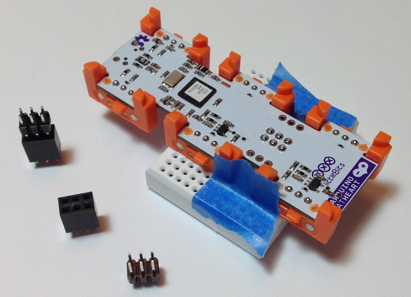
Music makers working with littleBits Arduino will almost certainly want to add a high(er) resolution digital-to-analog converter (DAC) to their Arduino. Part 1 shows how to add an ICSP header to your littleBits Arduino module. The ICSP header is where you find the SPI signals — MISO, MOSI, and SCK — along with Vcc (+5 Volts) and ground. The ICSP header pin layout is:

         GND ---O  O--- RESET
    MOSI/D16 ---O  O--- SCK/D15
         VCC ---O  O--- MISO/D14

This is the layout when viewing the top of the Arduino module with the USB connector at the top (i.e., away from you, “north” on a map).

Now let’s take a look at a simple circuit using the Microchips MCP4921 12-bit DAC. (Click on images to get higher resolution.)

spi_dac_schematic

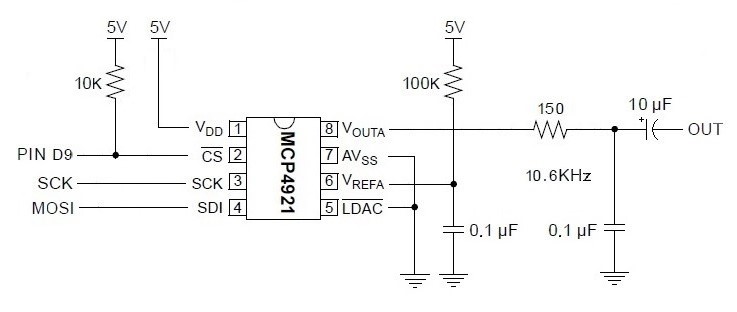
Three signals control the DAC: Slave Select (SS/Pin D9), Master Out Slave In (MOSI) and Serial Clock (SCK). Data is sent to the DAC through SPI’s bit serial protocol. First, SS is driven LOW, then 16 bits are sent one at a time to the DAC. SCK synchronizes the data bits sent via MOSI. The first byte consists of a 4-bit “command” and the top 4 bits of the 12-bit value to be converted. The second byte is the lower 8 bits of the value to be converted. After sending 16 bits, the SPI master drives SS HIGH. If you’re curious about all of the signaling details, please see the MCP4921 data sheet.

The rest of the DAC circuit consists of a voltage reference for the converter and a post-conversion (reconstruction) filter. The filter is a simple, one stage passive low pass filter with a 10,600Hz corner frequency.

I built the DAC circuit on a small solderless breadboard. Here’s the layout.

spi_dac_breadboard

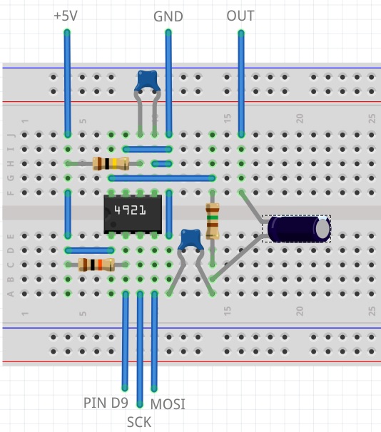
I connected MOSI, SCK, +5V and ground to the appropriate ICSP pins on the Arduino module. Slave Select is sourced by Arduino pin D9. I connected a littleBits Proto module to D9 and routed the input signal to the breadboard. If you want to postprocess the DAC’s audio output with littleBits modules, then route the DAC output to the Proto module’s output snap. Be sure to remove the shorting block (jumper) between the middle two pins on the Proto module. This approach provides power and ground to the audio postprocessing modules connected to the output snap of the Proto module — an important side-benefit.

The choice of pin D9 for Slave Select was the beginning of a long, hard journey in debugging. To make a long story short, pins D5 and D9 are buffered and the output buffer introduces additional delay on the Slave Select signal. The delay is long enough such that the DAC does not see a low Slave Select signal before data bits start arriving.

Here’s the code that writes the DAC:

#define NOP asm volatile ("nop\n\t")
void busyWait(uint8_t count) { 
  for(uint8_t i = count; i > 0 ; i--) { NOP ; } 
}

void writeDac(int16_t dacValue) {
  byte data ;
  SPI.beginTransaction(SPISettings(20000000,MSBFIRST,SPI_MODE0)); 
  digitalWrite(SlaveSelect, LOW) ;
  busyWait(25) ;
  data = highByte(dacValue) ;
  data = 0x0F & data ;
  data = 0x30 | data ;
  SPI.transfer(data) ;
  data = lowByte(dacValue) ;
  SPI.transfer(data) ;
  digitalWrite(SlaveSelect, HIGH) ;
  SPI.endTransaction() ;
}

The busy wait effectively stops the sketch for a little while after driving Slave Select LOW. This gives the Slave Select more time to reach the DAC before the sketch transfers the first data byte to the DAC. If you use an unbuffered pin like D1, you don’t need the busy wait.

It took a long time to eliminate all of the other possible issues that could have caused a failure: bad solder joints, wiring mistakes, etc. Fortunately, I have a similar DAC — the MidiVox — which works correctly. I also tested the hardware with Arduino UNO where all digital pins are unbuffered. It was frustrating to get everything working with the UNO, but not the littleBits Arduino module! Persistence wins the day.

In closing, I want to warn developers who interface high speed logic to littleBits Arduino. Beware of the delay through those buffered outputs! The delay may be long enough to throw off critical timing.

Add SPI to the littleBits Arduino

As Moe Szyslak might say, “He ain’t pretty no more!”

Last time through, I mentioned that I wanted to add a SPI digital-to-analog converter (DAC) to the littleBits Arduino module. The Microchips MCP4921 is a good candidate. It is a 12-bit DAC which communicates via the Small Peripheral Interface (SPI) bus or “SPI.”

The littleBits Arduino module is essentially an Arduino Leonardo. As such, its SPI port is available through the module’s ICSP pads. (“ICSP” stands for “in-circuit serial programming,” by the way.) The ICSP pads are the group of pads (two rows of three pads) between the D5 and D9 bitSnaps.

I soldered a 2×3 vertical pin header to the ICSP pads using a very simple jig. The image below is a “before and after” picture. (Click images for higher resolution.) The jig is a solderless breadboard that holds the header in place. I pushed the header into the breadboard just enough to hold the header and then placed the Arduino module over the header and pressed down. The idea is to get the black base of the header in contact and properly aligned with the module printed circuit board (PCB). The blue strips of masking (painter’s) tape keep the assembly together. The “after” part of the image shows the module with the header soldered in place.

icsp_solder_after

The jig really makes the soldering job easy. I have used other methods like trying to tape the header pins in place, but this approach was a piece of cake and frustration free.

The image below shows the header, module and jig just before soldering. The picture also shows the 2×3 vertical pin header and a compatible 2×3 female header block. You could install the female header block instead. I went with the male header because most ICSP cables expect a male header on the PCB to be programmed.

icsp_solder_jig

I ordered the parts from Mouser Electronics. Mouser and Jameco are my usual “go to” sources for components and tools. Here are the part numbers:

  • Harwin M20-9980346 03+03 DIL VERTICAL male header 2.54mm
  • Harwin M20-7830342 03+03 DIL VERTICAL female header 2.54mm
  • BPS BB170-WH White 170 point solderless breadboard
  • BPS ZW-MF-20 ZIPWIRE Female-Male 20cm
  • BPS ZW-MM-20 ZIPWIRE Male-Male 20cm

The “2.54mm” refers to the pin spacing (AKA “0.1 inch”). The female header is $1.19 and the male header is $.24. Buy at least ten of each and the price goes down a little. The contacts are tin; gold is a little more expensive.

I plan to make (eventually) little PCB “hats” using the female header blocks. The idea is to build a small, single-purpose circuit that plug onto the ICSP header or littleBits Proto module header like a hat. This approach would eliminate point-to-point connections using jumper wires. I may experiment with this approach once I get the basic DAC circuit ironed out and tested.

I really like Busboard Prototype System (BPS) products. BPS has the most useful prototyping board patterns. They also have these nifty ZIPWIRE ribbon cables. The wires terminate with individual male pins or female receptacles. Let’s say you need to make six connections from the ICSP header to a solderless breadboard. Then tear off a group of six wires and associated terminations. Push the receptacles onto the male header and push the pins into the solderless breadboard. The individual wires are color-coded in order to make the correct point-to-point connections at both ends. I’ll use ZIPWIRE to connect the Arduino SPI port (ICSP) to a solderless breadboard with the SPI DAC circuit.

If you have a littleBits Arduino module and want to make the most of it, it’s time to break out the soldering iron. Best of luck!

Beat Box at littleBits!

Apologies in advance as I spend more time remembering to be a musician, not a technology blogger. I bought a few MIDI files during the last Yamaha Musicsoft sale and I’m massaging them into PJ-approved backing tracks. Plus, I’m learning about the joys of the key of D-flat!

I posted the Beat Box drum machine project to the littleBits invention site. The littleBits project format is more “step-by-step” than the document that I post on this site. The step-by-step directions should help anyone interested in building the Beat Box without diving into the details of the design. Of course, you can still check out the Beat Box design at this site, too. (MP3 Demo)

Just so you don’t think I’ve been totally idle, I tried adapting the code to sing “Do-Re-Mi” solfege. This involved recording and editing my voice. I used my old trick of singing through the Yamaha PSR-S950 vocoder in order to pitch correct my rocky intonation. I had to lower the sample rate to 11,025Hz in order fit all eight syllables into the very small Arduino program memory (PROGMEM). Unfortunately, I cannot get clear audio at 11,025Hz. There is this raucous buzz which cannot be eliminated through filtering. I suspect that the problem is in the PWM generation itself. The waveforms play back fine at 22,050Hz, sounding like chipmunk solfege.

After hitting that brick wall, I’ve decided to take a different approach which has better long term possibilities. I’ve ordered a handful of MCP4921 12-bit SPI DAC ICs and intend to try them with the littleBits Arduino module. The littleBits Arduino is a Leonardo where the SPI interface is the (unpopulated) ICSP pads. The new approach requires soldering, but it should be worth the effort. Stay tuned.

Still tempted by the Reface CP and YC. But, $400USD street? C’mon, Yamaha!

Inside Reface DX and Reface CS

With so much to do and learn, it’s been a long while since I’ve taken a peek below the hood of an electronic musical instrument.

Yamaha caught the world by surprise with its Reface series of portable keyboards. So far, there are four models in the series: Reface YC (organ), Reface CP (electric piano), Reface CS (analog modeling synthesizer), and Reface DX (4-op FM synthesizer).

Before I get to the DX and CS, here’s a few thoughts about the YC and CP. According to Yamaha specifications, the Reface YC tone generation engine is “AWM (Organ Flutes)”. This suggests to me that the YC uses a standard AWM tone generation integrated circuit (IC) like the SWP70. Hammond-like “Organ Flutes” have been part of the mid- and upper-tier arranger workstations like Tyros for a very long time. Thus, I suspect that the YC implementation is an updated implementation of the arranger technology.

The Reface CP tone generation engine is specified as “SCM + AWM2”. SCM or “Spectral Component Modeling” is the modeling technique first employed in the flagship CP-1 stage piano. SCM and AWM2 are also used in the CP-4 and CP-40 models. The CP-1 uses three tried-and-true SWP51L tone generation ICs: master, slave and effects. The master and slave generate the base piano tones and the two ICs share the same WAVE ROM. Total WAVE ROM size is 1024Mbits or 128MBytes (organized as 16-bit words) which is a ridiculously small amount of memory for a top quality piano. Such is the power of SCM!

The CP-1’s samples are stored in two Lapis Semiconductor MR26V51252R devices (32M by 16-bit words each). The processor is a Yamaha SWX02 (SH-2A CPU core operating at 135.4752MHz). There’s not much to the CP-1 user interface, so a relatively light-weight, low-cost processor is enough for the job. The SWP51Ls handle all of the heavy computation.

Thus, the Reface YC and Reface CP are relatively uninteresting from a technologist’s point of view. The YC and CP use proven technology from other Yamaha products. That leaves the Reface CS and Reface DX.

Although the CS and DX implement two different tone generation techniques — analog physical modeling vs. frequency modulation (FM) — they are fraternal twins at the hardware level. They share much of the same base hardware design with a few variations to handle their unique user interface requirements.

The CS and DX both use a Fujitsu MB9AF141LAPMC1 processor to handle key and panel scanning. Here’s a quick summary of its characteristics:

    CPU                 Cortex-M3
    CPU Frequency       40MHz

    On-chip flash memory   Main area   64KBytes
    On-chip flash memory   Work area   32KBytes
    On-chip SRAM           SRAM0        8KBytes
    On-chip SRAM           SRAM1        8KBytes

    Peripheral interfaces:
        DMAC            8 channel
        Serial I/F      8 channel
        Base timer      8 channel
        Dual timer      1
        Realtime clock  1
        Watch counter   1
        12-bit A/D      12 channel

This processor is a good choice for embedded control applications where low power and low cost are important. To my knowledge, this is the first product line using an ARM embedded microcontroller.

The Reface CS and Reface DX both use the proprietary Yamaha SSP2 (uPD800500F1-011-KN9-A) for tone generation. The SSP2 is Yamaha’s designated hitter for DSP tasks and is incorporated into many products. The SSP2 has an SH-2A CPU core operating at an internal clock speed of 135.4752MHz. The SSP2 has its own ADC, GPIO, UART, USB and serial audio interfaces. The SSP2 UART handles 5-pin MIDI communications. The SSP2 USB interface handles external USB communications.

The SSP2 has two memory interfaces:

  • DSP RAM: Connecting to 8MBytes of DSP SDRAM.
  • CPU bus: Connecting to 8MBytes of program ROM and 16MBytes of SDRAM.

Memory sizes and devices are the same in both products.

The AUX IN and audio out hardware design is also the same across the two products:

  • PCM1803ADBR ADC: AUX IN analog-to-digital converstion
  • AK4396: Digital-to-analog conversion for OUTPUT L/R and PHONES OUT
  • YDA176 D-Amp: DAC and amplification for internal speakers

This shouldn’t be any surprise. All of the Reface series products ahare the same external jack, power and key switch boards.

Digital audio is transfered serially between the SSP2, the ADC, the DAC and the digital amplifier. The SSP2 generates the master clock (MCLK) and bit clock (BCLK) to synchronize data transfers. MCLK and BCLK are derived from the SSP2 clock, in case you’re wondering about those odd-looking CPU clock frequencies. MCLK is 256*fs and BCLK is 64*fs, where fs is the sampling frequency, 44.1KHz. MCLK operates the AK4396’s digital interpolation filter and delta signal modulator. Data format is I2S and is probably 24-bit as it is in workstation products.

Aside from the other front panel controls, the Reface DX has two major additions: Capacitive sensors for the front panel touch strips and the LCD panel display. The printed circuit board positions for the LCD interface are not populated (i.e., no mount) in the Reface CS as it has no LCD display.

There you have it — two more examples of solid and conservative Yamaha hardware design.

Now, you may find the SSP2 to be incredibly boring. It is, however, a good choice for a low-cost, compact product. The Reface CS and DX need a metal shield over the SSP2, perhaps to control RF emissions, perhaps to radiate heat, or maybe both purposes together. Low power is a vital concern throughout the Reface series due to battery power concerns.

I’m a little hesitant to draw any inferences about future products. The Yamaha Montage supports 128 note, 8 operator FM polyphony. The Reface DX provides a relatively meager 8 note, 4 operator FM polyphony. Thus, there must be considerable hardware resources at work in the Montage. Well-worth the price, one hopes! And speaking of hopes, many people would like an analog modeling extension to the Montage. That would depend, of course, on the availability of spare computational horsepower.

Copyright © 2016 Paul J. Drongowski