
Now let’s take a first look at Yamaha PSS-E30 Remie inside.
My Remie is a seasoned world traveller. It was designed in Japan, made in India, distributed by Rellingen, Germany, sold by Amazon UK and played in Washington state, USA. Physics and electrons are indeed universal.
The PSS-E30, PSS-F30 and PSS-A50 are essentially the same physical product. They are part of a family like Reface. The Reface family, BTW, is two pairs of fraternal twins: YC/CP and CS/DX. The PSS family are fraternal triplets and share the same printed circuit board (PCB). In fact, the PCB has three little check boxes. A mark in a check box denotes the specific product personality.
Product personality is determined by four things: front panel graphics, software, content (voices, styles, etc.) and USB interface.
Line up the three PSS keyboards and you see that they all have the same panel layout. The buttons are all in the same physical place. Everything else that is external is just skin (case color and stick on panel graphics). The panel connections to the digital logic board (DM) are the same in all three products.
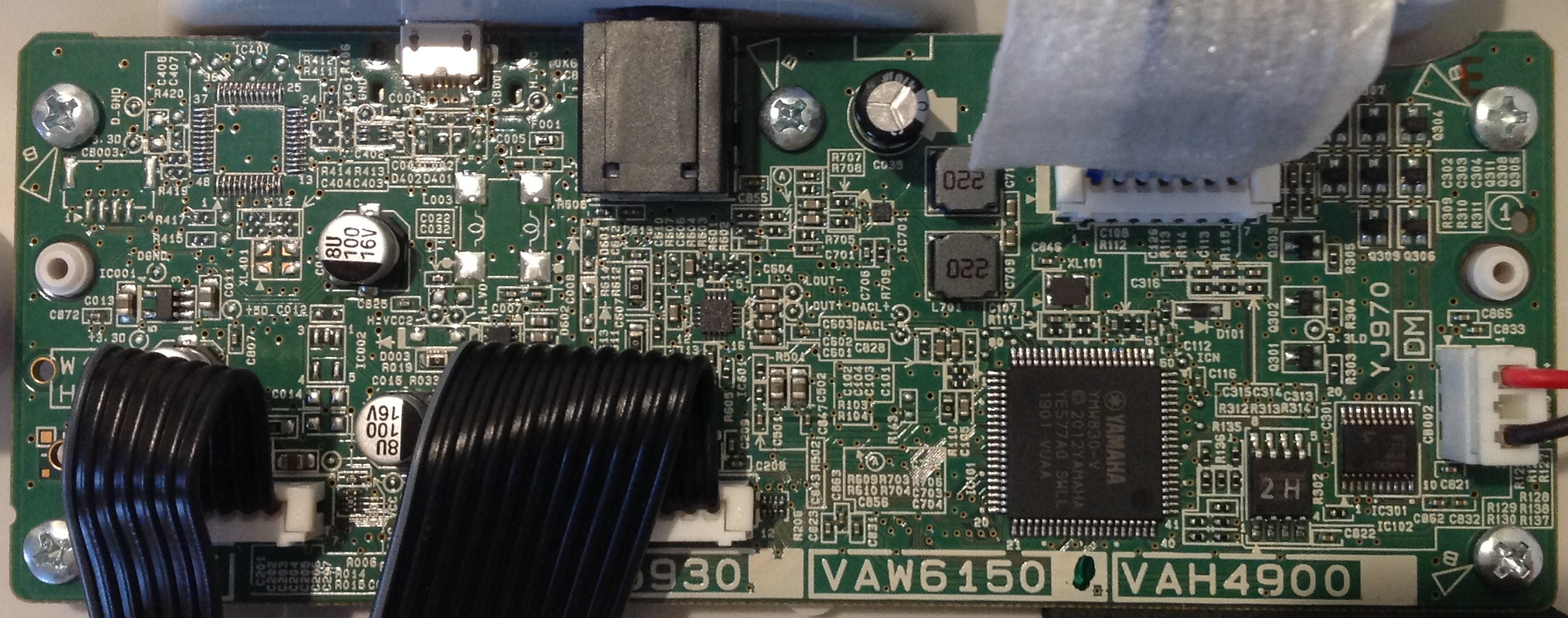
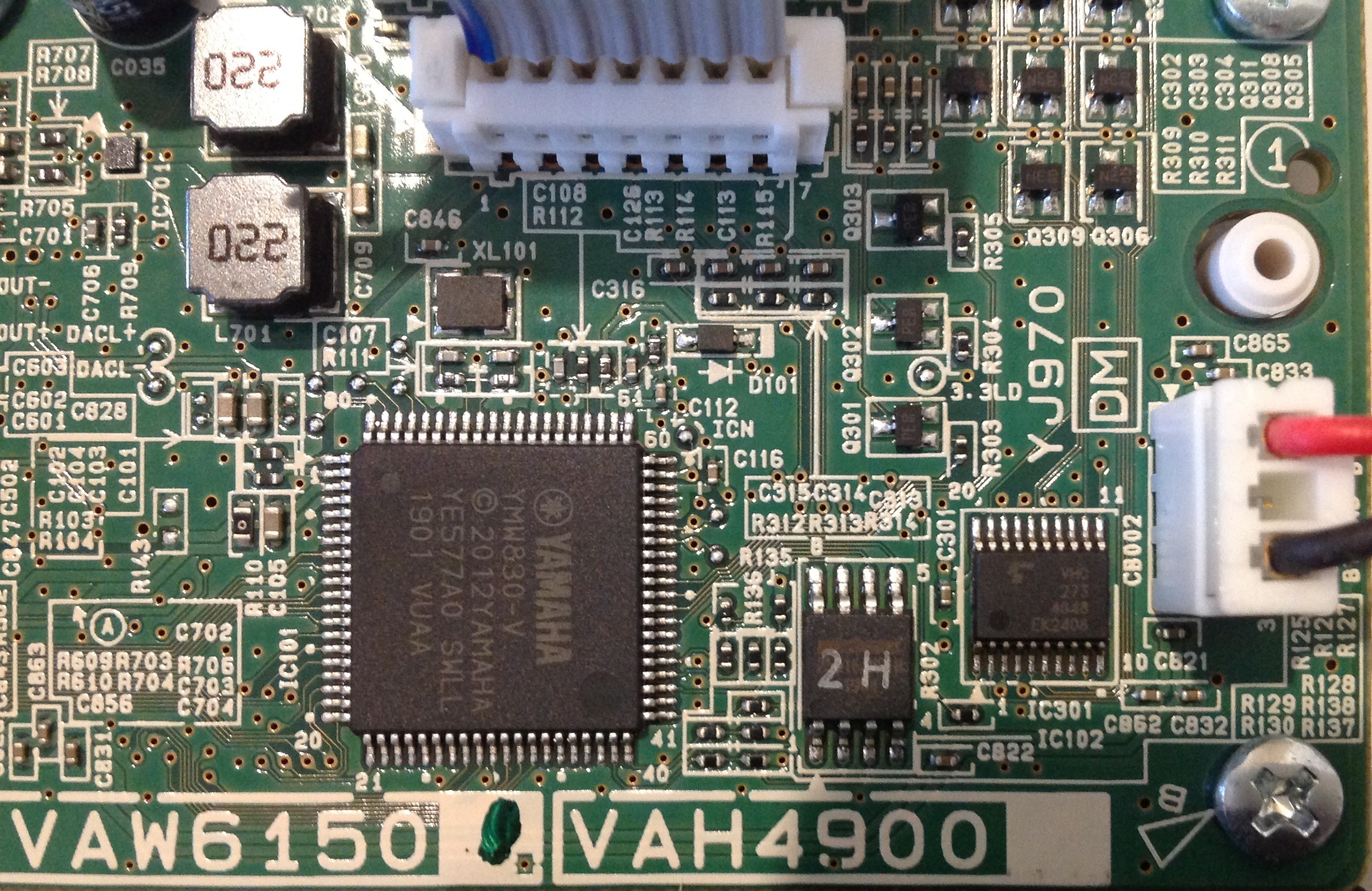
Next up, each member of the family has different code and content. The software and content are stored in a Winbond 2MByte serial ROM. The main CPU (SWLL) reads the binary code and waveforms from ROM at boot time. The ROM components are stamped with a product specific code: “2H” for Remie and “2I” for the PSS-A50.
The 2MByte ROM holds both code and waveforms. The small ROM harkens back to the day of the Yamaha QY-70 when XG voices and drum kits fit into 4MBytes. Given the small ROM, one shouldn’t expect super high voice quality in any of the models.
The SWLL is reminiscent of the YMW-820 NSX-1 integrated circuit. The NSX-1 is the engine behind Pocket Miku and eVocaloid.
Finally, the PSS-A50 is the only sibling with an active USB interface. Remie has an unpopulated IC site as you can see in the upper left corner of its PCB. This site is populated with a USB chip in the A50. Without the chip, Yamaha can build and sell Remie at a lower cost than the A50. Even if one carefully soldered the correct USB IC into the unpopulated site in Remie, I doubt if Remie’s software has the code to recognize it.
The PSS-F30 is a shrunken PSR-F50. For the rest of this discussion, I’m using the Yamaha PSR-F50 Service Manual as my guide to the electronics. As to the keybed, I’m using the Reface YC Service Manual.
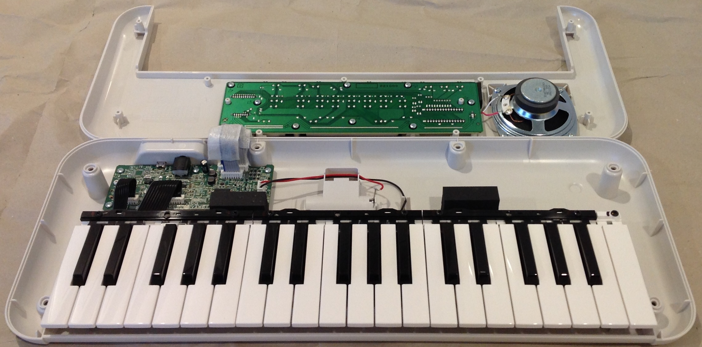
Inside, each member of the PSS family consists of three circuit boards: the main logic board (DM), the front panel board and the keybed. The front panel board and keybed are each a switch matrix. The CPU scans both the front panel and keybed separately. It scans each board by asserting a switch group select signal and then reading the current state of each switch in the group.
There are twelve switches in a keybed group, two switches per key. The switch contacts are at two different heights and close at two different times when struck. The CPU measures the closure time between the first contact and the second conent in order to sense key velocity.
The panel PCB and the keybed PCB are each joined to the digital logic board by short ribbon cables. The loudspeaker signals hitch a ride through the front panel ribbon cable.
The main CPU and tone generator is a Yamaha proprietary integrated circuit — the YMW830-V or “SWLL”. The SWLL is the ultra-small brother to the SWL01. The chip is housed in an 80 pin surface mount quad pack which is only 1.3cm on a side. That’s tiny. The entire PCB is a tidy 13.5cm by 4.5cm.
The SWLL is a true system on a chip (SOC) containing the CPU, RAM, tone generation circuitry, UART, ADCs and DACs. Amazing. The chip inside is small, too, and Yamaha can print these like postage stamps in large volume. Everything about the SWLL screams “low cost”.
Using the PSR-F50 Service Manual, here is the SWLL pin-out:
     1   DACLPP    Left channel DAC output (positive)
     2   DACLMM    Left channel DAC output (minus)
     3   DAC_VDD   DAC Vdd
     4   DAC_VSS   DAC Vss
     5   DACRMM    Right channel DAC output (minus)
     6   DACRPP    Right channel DAC output (positive)
     7   VSS       Vss
     8   KYN11     Key sense (input)
     9   KYN12     Key sense
    10   KYN13     Key sense
    11   KYN14     Key sense
    12   KYN15     Key sense
    13   KYN16     Key sense
    14   KYB1      Keyboard key group select (output)
    15   KYB2      Keyboard key group select
    16   KYB3      Keyboard key group select
    17   KYB4      Keyboard key group select
    18   KYB5      Keyboard key group select
    19   KYB6      Keyboard key group select
    20   KYB7      Keyboard key group select

    21   KYB8      Keyboard key group select
    22   KYB9      Keyboard key group select
    23   KYB10     Keyboard key group select
    24   KYB11     Keyboard key group select
    25   IOVDD
    26   VSS
    27   LDOTSTO
    28   KYN21     Key sense (input)
    29   KYN22     Key sense
    30   KYN23     Key sense
    31   KYN24     Key sense
    32   KYN25     Key sense
    33   KYN26     Key sense
    34   SWIN0     Panel scan input
    35   SWIN1     Panel scan input
    36   SWIN2     Panel scan input
    37   SWIN3     Panel scan input
    38   VSS
    39   SDQ2      Serial ROM WP# (DQ2)
    40   SDO       Serial ROM DO (DQ1)

    41   SCSN      Serial ROM chip select (CS#)
    42   IOVDD
    43   SDQ3      Serial ROM NC (DQ3)
    44   SCLK      Serial ROM clock (CLK)
    45   SDI       Serial ROM DI (DQ0)
    46   VSS
    47   PORTB0    PSW0
    48   PORTB1    (7seg_e0)
    49   PORTB2    (7seg_e1)
    50   PORTB3    (7seg_e2)
    51   PORTB4    (7seg_lat)
    52   PORTE0    /PSWI
    53   PORTC0    (Sustain input)
    54   TXD       UART transmit data (output)
    55   RXD       UART receive data (input)
    56   PLLBP
    57   TEST
    58   LDOTST
    59   IC_       (Voltage detector)
    60   VSS

    61   ADC_VDD   (+3.3V)
    62   ADC_VSS   (Ground)
    63   AN0       Analog input
    64   AN1       Analog input (battery check)
    65   VSS
    66   PLLVSS
    67   PLLVDD
    68   LDOC
    69   LDOVDD
    70   LDOVSS
    71   VSS
    72   XI        Crystal input
    73   XO        Crystal output
    74   VSS
    75   IOVDD
    76   TDO       Test data out
    77   TCK       Test clock
    78   TMS
    79   TDI       Test data in
    80   TRST_     Test reset
I determined pin function by tracing signals in the PSR-F50 Service Manual. Yamaha may have changed things a bit in Remie and A50. I have not determined how the USB interface is connected to SWLL in the A50 nor have I even identified the component.
For the PSR-F50, the SWLL internal clock is 33.8688MHz and the master clock is 67.7376MHz. The clocks are generated from a 16.9344MHz crystal. All clocks are a multiple of 44,100Hz, the sample frequency. I can’t read the marking on Remie’s crystal, but there isn’t any reason to believe that it differs from F50.
The three digit LED display is both retro and cheap. Remie has the same eleven transistors driving the time-multiplexed seven segment display.
- Under software control, transistors Q301 to Q303 (7seg_e0 to 7seg_e2) select one of the three digits.
- Transistors Q304 to Q311 drive the individual segments.
Segment status is latched into an eight flip-flop SN74LV273 from the SWL KYB1 to KYB8 pins. The latch clock is produced by SWLL pin PORTB4 (7seg_lat). Note that the KYB pins do double duty as inputs from the keybed.
Whew! That leaves us deep in the weeds! Next time, I’ll outline a few ways to mod the new PSS keyboards.
Update: Compare Remie against my Yamaha PSS-A50 teardown.
Copyright © 2019 Paul J. Drongowski