Kawai MP11: Digital electronics

Let’s take a brief look at the electronics inside the Kawai MP11 digital piano.

The Kawai MP11 is a pro-level 88-key stage piano with Grand Feel wooden key action and triple sensor detection. The MP11 has 40 voices total including Kawai concert and studio acoustic pianos, electric pianos and the usual motley crew of non-piano voices. Acoustic pianos are enhanced by Kawai’s Harmonic Imaging™ XL technology. 23 different kinds of effect can be applied. Electric piano gets special treatment with five amp simulators: Suitcase, Marshall stack, Jazz Chorus, Bassman and Leslie. The MP11 Virtual Technician allows control of tonal character, stereo width, string resonance, etc.

The MP11 has pitch bend and mod wheels, key set-ups (zones), assignable knobs, and many other features that make it suitable as a controller. It also has sought-after features like built-in power supply (no wall wart), 5-pin MIDI, XLR audio OUT.

That’s one respectable stage piano!

Having crawled through many service manuals before, the internals are not too surprising. There is one main digital electronics board surrounded by several peripheral boards for the LCD (128×64), USB interface, front panel gizmos, audio amplification, and various external connections. There are separate boards for handling AC main power.

Kawaii MP11 block diagram [Kawai service manual]

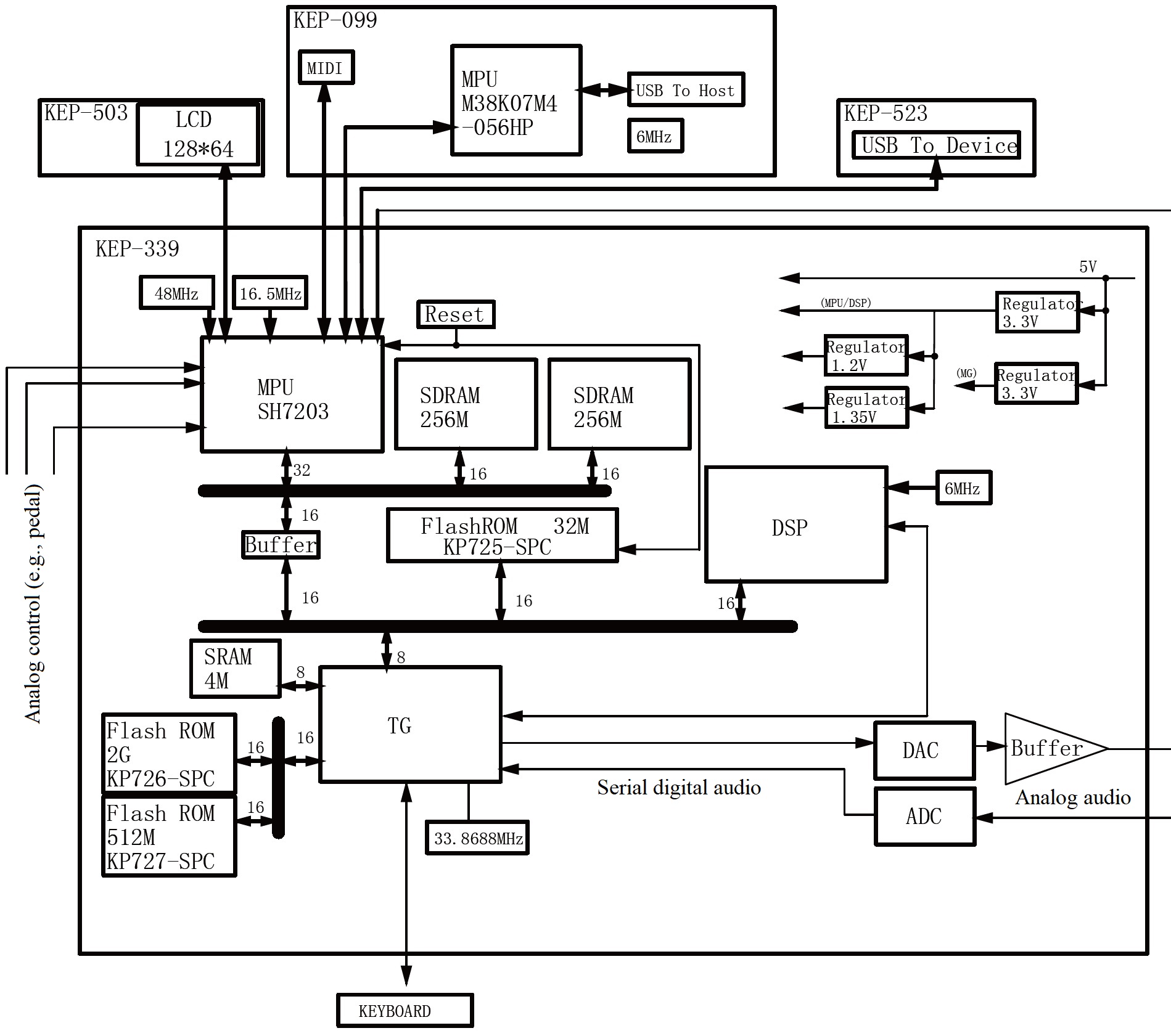
I’m most interested in the on-board compute and, thus, I will focus on the main logic board. Like other high-end digital synthesis products (e.g., Yamaha Montage), there are multiple hardware processors. The MP11 has three main processors:

  • Main CPU (MPU): Renesas SH7203
  • Tone Generator (TG): unspecified by the service manual
  • Effects (DSP): unspecified

Unfortunately, the Kawai service manual does not provide a detailed schematic or electrical parts list. Thus, the TG and DSP type are unspecified by the service manual. The DAC and ADC are unspecified, too. A fourth processor, Renesas 8-bit MPU M38K07M4, handles USB to HOST duties.

The MPU is the well-known Renesas SH7203, a 32-bit microcontroller incorporating an SH2A FPU RISC core. There are two external clocks: 48MHz and 16.5MHz. The 48MHz oscillator is probably the USB clock. The 16.5MHz clock is multiplied internally according to the software-configured frequency control register. The SH7203 can operate up to 200MHz internally.

The MPU has two 32 MByte SDRAMs (type unspecified), for 64 MBytes total. The MPU shares a 4 MByte flash ROM with the TG and DSP processors. Data moves in 16-bit words.

An arty, notional Kawai K023-FP IC [Kawai]

The tone generator, TG, has a 33.8688MHz external clock. The clock is an even multiple of 44.100kHz, the outgoing sample frequency. I suspect that the DAC and ADC employ the standard I2S serial communication protocol for digital audio. Thus, TG has 768 clock cycles to knock out a single N-bit sample to go to the DSP effect unit or the DAC.

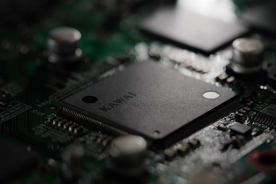
Tear down videos such as the Kawai CN23 disassembly reveal Kawai proprietary tone generation integrated circuits (IC). The IC in the CN23, for example, is a massive, 208-pin beast!

TG has a small working SRAM (512MB, 8-bit data path, type unspecified). TG has two dedicated flash ROM devices (type unspecified) for TG program and waveform (sample) storage: 256 MBytes and 64 MBytes. Waveform data moves on 16-bit paths.

This MP11 repair video shows a large custom IC: Kawai K023-FP. There is another custom IC on the main logic board. Which one is sh7203? TG? DSP? It’s clear that Kawai design their own ICs.

The DSP unit has a relatively leisurely 6MHz clock. The DSP unit receives digital audio from the TG and returns it to TG, DSP does not have a direct connection to the DAC.

The MP11 has a LINE IN for external audio. The LINE IN is buffered and then converted to digital audio by the ADC (type unspecified). The digital audio stream goes to TG where it is mixed digitally with synthesized audio.

Armed with other tear down videos and resources on the Web, I’ll try to identify these unspecified MP11 components.

  • Main CPU: Renesas 72030W200FP (package QFN-240, 240 pins)
  • MPU SDRAM: Elite Semiconductor Memory Technology ESMT M12L25616A-6T 256Mbit SDRAM organized as 16M x 16-bit words
  • TG: Kawai K023-FP identified in another Kawai service manual as “Sound Source/Touch LSI”
  • Flash ROM: Generic NOR flash organized as N x 16-bit words (e.g., Spansion S29GL01GP12TFI020); Flash ROM ICs have Kawai labels identifying pre-loaded content
  • TG SDRAM: Infineon CY7C1049DV33 4Mbit fast async SRAM organized as 512K x 8-bit bytes
  • DSP: Texas Instruments TMS320VC5507 Fixed-point Digital Signal Processor

As to DAC, Kawai have used the Asahi Kasei AKM 4490EQ 32-bit DAC and Texas Instruments PCM1795 in previous products. I wonder how Kawai have coped while AKM recover from their factory fire? Perhaps they are using the ESS Technology ES9028Q2M 32-bit DAC instead?

If you see a photo of the Kawai KEP-339 main board, you are probably looking at the top side only. Please keep in mind that the bottom side is also populated. You will find the TI TMS320 DSP on the bottom side.

Folks are always surprised by the modest compute resources in digital keyboards. They expect to see giga Hertz clock speeds, gobs of memory and solid state storage devices (SSD). Synth engines are so-called embedded systems, not desktop workstations or laptops. The digital electronics need to run cool without heavy heatsinks and fans. In order to achieve power/heat goals, clock rates are low and basic memory interfaces are employed instead of PC busses such as SATA.

Hope this short tour is informative!

Copyright © 2023 Paul J. Drongowski

Digital piano: Tear the roof off

Long-term readers know that my mind will eventually turn to tear-downs and electronics. So it goes with digital pianos.

Thanks to the Piano World Forum, I found two links of interest to deep divers.

Inside Yamaha P-515

First up is a long-ish Yamaha P-515 repair video. I’ve got to say, tearing down a P-515 is not for the faint-hearted. We owe Late Night DIY much gratitude for taking the challenge.

I’d loved to include some screensnaps here, but Late Night’s camera work is a little shaky. (Dude shot the video after a late night gig.) Here is a list of things to watch for:

  • 5:14: Particle board base.
  • 6:57: The AJACK board with external connectors.
  • 7:51: The keybed.
  • 8:17: Rubber contact strips.
  • 9:47: Contact PCB traces.
  • 11:10: Key removal.
  • 24:11: Speaker box.
  • 25:16: AJACK, again. DM board is underneath.
  • 27:07: Top of speaker box.

These camera shots should give you a pretty good tour of the insides without going through the whole disassembly and repair narrative.

Disassembly tips: Take pictures while ripping things apart. Mark holes on printed circuit boards. Do not put screws and other hardware in speaker cones!

A few observations. First, look at the size of the particle board base! The wood base provides strength and rigidity for the NWX keybed. The base must weight at least ten pounds. Think about that when hefting your P-515 around.

The AJACK printed circuit board (PCB) has all of the MIDI and audio connectors. The main PCB — the digital logic (DM) mainboard — is underneath the AJACK. I dearly wish we had pictures (top and bottom) of the DM mainboard.

The rubber contact strips beneath the keys have three nubby buttons for each key. The nubby buttons make contact with the PCB contact traces (those squiggly squares). This is the so-called “triple sensor.” Other than three contacts instead of two, the basic hardware tech ain’t different from digital synths. The hardware “sensor” isn’t that sophisticated as all of the smarts are in the scanning software.

The speaker box is cool. I wouldn’t be surprised to see it inside of P-S500, too. Yamaha reuses components to cut costs and spare parts inventory.

The speaker box and NWX key designs are probably patented. I am surprised that the Piano World folks haven’t exploited the U.S. PTO patent database…

Inside Yamaha CLP-685

Several posts on Piano World Forum cite this look into the Yamaha CLP-685.

More than a look, this is one of the most gutsy tear-downs that I’ve seen. Guy buys an expensive CLP-685 and literally takes it apart out of curiosity. I usually play with my toys before taking them apart and I rarely take apart anything over $100 USD retail. That’s some Chinese chutzpah!

This article has a lot of terrific pictures (some a little blurry, unfortunately). There are good close-up pictures of the tan power supply boards and the DMH main digital electronics board.

Yamaha CLP-685 digital piano main board (DMH)

I wish the DMH board legends were legible and I wish that we had a picture of the other side, too. Plain as day is a Yamaha SWX09 (YH621A0) integrated circuit. The SWX09 integrates the main CPU, tone generation and digital effects onto a single chip. I’ll be thinking about this more in days to come, especially the “empty” board real estate. The SWX09 has nearby companions. The Winbond W9864G6KH-6 4M by 16-bit 166MHz SDRAM is DSP working memory for the SWX09. The two labeled ICs are wave ROM. The rest of the components are mounted on the bottom of the board. We see only the components mounted on the top side of the board.

A Yamaha GrandTouch key

The Piano World Forum folk are positively obsessed with key design and action. Yamaha describe the CLP-685 keybed thus:

GrandTouch keyboard: Wooden keys (white only), synthetic ebony and ivory key tops, escapement

I see a lot of plastic, a metal weight, and a little decorative wood. I’m not hung up on wood vs. plastic as even Einstein would say “Dead mass is dead mass.” If it plays good, why worry? The only concern I have about anything is long-term durability (e.g., those rubber contact strips and dirt).

Hope other musical electronics nerds have found this exposition interesting. 🙂

Copyright © 2023 Paul J. Drongowski

Inside Yamaha PSS-E30 Remie

Now let’s take a first look at Yamaha PSS-E30 Remie inside.

My Remie is a seasoned world traveller. It was designed in Japan, made in India, distributed by Rellingen, Germany, sold by Amazon UK and played in Washington state, USA. Physics and electrons are indeed universal.

The PSS-E30, PSS-F30 and PSS-A50 are essentially the same physical product. They are part of a family like Reface. The Reface family, BTW, is two pairs of fraternal twins: YC/CP and CS/DX. The PSS family are fraternal triplets and share the same printed circuit board (PCB). In fact, the PCB has three little check boxes. A mark in a check box denotes the specific product personality.

Yamaha PSS-E30 Remie digital logic board (DM)

Product personality is determined by four things: front panel graphics, software, content (voices, styles, etc.) and USB interface.

Line up the three PSS keyboards and you see that they all have the same panel layout. The buttons are all in the same physical place. Everything else that is external is just skin (case color and stick on panel graphics). The panel connections to the digital logic board (DM) are the same in all three products.

Next up, each member of the family has different code and content. The software and content are stored in a Winbond 2MByte serial ROM. The main CPU (SWLL) reads the binary code and waveforms from ROM at boot time. The ROM components are stamped with a product specific code: “2H” for Remie and “2I” for the PSS-A50.

The 2MByte ROM holds both code and waveforms. The small ROM harkens back to the day of the Yamaha QY-70 when XG voices and drum kits fit into 4MBytes. Given the small ROM, one shouldn’t expect super high voice quality in any of the models.

The SWLL is reminiscent of the YMW-820 NSX-1 integrated circuit. The NSX-1 is the engine behind Pocket Miku and eVocaloid.

Finally, the PSS-A50 is the only sibling with an active USB interface. Remie has an unpopulated IC site as you can see in the upper left corner of its PCB. This site is populated with a USB chip in the A50. Without the chip, Yamaha can build and sell Remie at a lower cost than the A50. Even if one carefully soldered the correct USB IC into the unpopulated site in Remie, I doubt if Remie’s software has the code to recognize it.

The PSS-F30 is a shrunken PSR-F50. For the rest of this discussion, I’m using the Yamaha PSR-F50 Service Manual as my guide to the electronics. As to the keybed, I’m using the Reface YC Service Manual.

Remie circuit boards and ribbon cables

Inside, each member of the PSS family consists of three circuit boards: the main logic board (DM), the front panel board and the keybed. The front panel board and keybed are each a switch matrix. The CPU scans both the front panel and keybed separately. It scans each board by asserting a switch group select signal and then reading the current state of each switch in the group.

There are twelve switches in a keybed group, two switches per key. The switch contacts are at two different heights and close at two different times when struck. The CPU measures the closure time between the first contact and the second conent in order to sense key velocity.

The panel PCB and the keybed PCB are each joined to the digital logic board by short ribbon cables. The loudspeaker signals hitch a ride through the front panel ribbon cable.

The main CPU and tone generator is a Yamaha proprietary integrated circuit — the YMW830-V or “SWLL”. The SWLL is the ultra-small brother to the SWL01. The chip is housed in an 80 pin surface mount quad pack which is only 1.3cm on a side. That’s tiny. The entire PCB is a tidy 13.5cm by 4.5cm.

The SWLL is a true system on a chip (SOC) containing the CPU, RAM, tone generation circuitry, UART, ADCs and DACs. Amazing. The chip inside is small, too, and Yamaha can print these like postage stamps in large volume. Everything about the SWLL screams “low cost”.

Using the PSR-F50 Service Manual, here is the SWLL pin-out:

     1   DACLPP    Left channel DAC output (positive)
2 DACLMM Left channel DAC output (minus)
3 DAC_VDD DAC Vdd
4 DAC_VSS DAC Vss
5 DACRMM Right channel DAC output (minus)
6 DACRPP Right channel DAC output (positive)
7 VSS Vss
8 KYN11 Key sense (input)
9 KYN12 Key sense
10 KYN13 Key sense
11 KYN14 Key sense
12 KYN15 Key sense
13 KYN16 Key sense
14 KYB1 Keyboard key group select (output)
15 KYB2 Keyboard key group select
16 KYB3 Keyboard key group select
17 KYB4 Keyboard key group select
18 KYB5 Keyboard key group select
19 KYB6 Keyboard key group select
20 KYB7 Keyboard key group select

21 KYB8 Keyboard key group select
22 KYB9 Keyboard key group select
23 KYB10 Keyboard key group select
24 KYB11 Keyboard key group select
25 IOVDD
26 VSS
27 LDOTSTO
28 KYN21 Key sense (input)
29 KYN22 Key sense
30 KYN23 Key sense
31 KYN24 Key sense
32 KYN25 Key sense
33 KYN26 Key sense
34 SWIN0 Panel scan input
35 SWIN1 Panel scan input
36 SWIN2 Panel scan input
37 SWIN3 Panel scan input
38 VSS
39 SDQ2 Serial ROM WP# (DQ2)
40 SDO Serial ROM DO (DQ1)

41 SCSN Serial ROM chip select (CS#)
42 IOVDD
43 SDQ3 Serial ROM NC (DQ3)
44 SCLK Serial ROM clock (CLK)
45 SDI Serial ROM DI (DQ0)
46 VSS
47 PORTB0 PSW0
48 PORTB1 (7seg_e0)
49 PORTB2 (7seg_e1)
50 PORTB3 (7seg_e2)
51 PORTB4 (7seg_lat)
52 PORTE0 /PSWI
53 PORTC0 (Sustain input)
54 TXD UART transmit data (output)
55 RXD UART receive data (input)
56 PLLBP
57 TEST
58 LDOTST
59 IC_ (Voltage detector)
60 VSS

61 ADC_VDD (+3.3V)
62 ADC_VSS (Ground)
63 AN0 Analog input
64 AN1 Analog input (battery check)
65 VSS
66 PLLVSS
67 PLLVDD
68 LDOC
69 LDOVDD
70 LDOVSS
71 VSS
72 XI Crystal input
73 XO Crystal output
74 VSS
75 IOVDD
76 TDO Test data out
77 TCK Test clock
78 TMS
79 TDI Test data in
80 TRST_ Test reset

I determined pin function by tracing signals in the PSR-F50 Service Manual. Yamaha may have changed things a bit in Remie and A50. I have not determined how the USB interface is connected to SWLL in the A50 nor have I even identified the component.

Yamaha PSS-E30 Remie LSI components

For the PSR-F50, the SWLL internal clock is 33.8688MHz and the master clock is 67.7376MHz. The clocks are generated from a 16.9344MHz crystal. All clocks are a multiple of 44,100Hz, the sample frequency. I can’t read the marking on Remie’s crystal, but there isn’t any reason to believe that it differs from F50.

The three digit LED display is both retro and cheap. Remie has the same eleven transistors driving the time-multiplexed seven segment display.

  • Under software control, transistors Q301 to Q303 (7seg_e0 to 7seg_e2) select one of the three digits.
  • Transistors Q304 to Q311 drive the individual segments.

Segment status is latched into an eight flip-flop SN74LV273 from the SWL KYB1 to KYB8 pins. The latch clock is produced by SWLL pin PORTB4 (7seg_lat). Note that the KYB pins do double duty as inputs from the keybed.

Whew! That leaves us deep in the weeds! Next time, I’ll outline a few ways to mod the new PSS keyboards.

Update: Compare Remie against my Yamaha PSS-A50 teardown.

Copyright © 2019 Paul J. Drongowski

Yamaha MODX: Inside stuff

Time for a quick look at the MODX internal hardware. I’m going to be brief, so please read my Yamaha Genos articles (main CPU and tone generation) and my Montage internals article for more details and background information.

The MODX main CPU subsystem should look familiar. It is essentially the same as the Montage main CPU subsystem. Again, the Texas Instruments AM3352 Sitara ARM microprocessor is the star, providing many of the important internal device interfaces. The eMMC bulk storage device is still 4GBytes although the MODX eMMC data clock is slightly slower than Montage (48MHz instead of 52MHz). Deja vu all over again.

MODX Main CPU (Click to enlarge)

The MODX is a reduced-spec Montage. Although the MODX has the same waveforms and Performances as Montage, its polyphony is less:

  • AWM2: 128 (maximum; stereo/mono waveforms)
  • FM-X: 64 (maximum)

The keybed is lower quality (semi-weighted vs. FSX) and the MODX front panel is greatly simplified.

Both products employ an MB9AF141NA ARM microcontroller for user interface scanning assisted by an 89FM42AUG logic device (E-GKS) for keybed scanning. User input (e.g., controller messages) are sent to the Master SWP70 tone generator over the EBUS. The EBUS is a low-latency path for controller input and commands, making for a responsive instrument with excellent hand-to-sound connection.

MODX Tone Generation (Click to enlarge)

When we look at the MODX tone generation subsystem, we immediately see why the FM-X spec is lower. The MODX has only one SWP70 tone generator integrated circuit (IC). The Master SWP70 performs both AWM2 and FM-X synthesis. The MODX printed circuit board (PCB) has space and connections for a second SWP70 (in Slave mode), but the real estate is unpopulated (“No Mount”). Yamaha have planned ahead for a future model. They did the same thing with the MOX, BTW, leaving space and connections that were filled in the MOXF.

The extra computational capacity within a single SWP70 is surprising! The Master SWP70 provides 128 channels of AWM2 polyphony and 64 channels of FM-X polyphony. In order to pull off this trick, Yamaha utilize a second dedicated DSP RAM channel and SDRAM. Montage, on the other hand, utilizes only one DSP RAM channel on each SWP70.

Thus, the SWP70 can expand in two different dimensions:

  • DSP RAM (two dedicated channels max) with a corresponding boost in DSP computation, and
  • Wave RAM (two dedicated channels max) with an as-yet unexploited boost in AWM2 synthesis.

MODX illustrates the first case while Montage has an unpopulated position and connections for a second WAVE working memory channel. Your guess is as good as mine as to how Yamaha will expand and exploit these channels in future products.

The MODX serial digital audio bus is a subset of Montage. An SSP2 processor supports audio-over-USB through the USB TO HOST interface, just like Montage. However, the overall spec is substantially reduced. A single DAC drives the MAIN and PHONE outputs. A single ADC encodes incoming stereo audio from the A/D input. The SSP2 does not have a direct channel to an SSP2; the needed logic device is missing from MODX.

In case you’re wondering about serial audio bus clocking, the bus clock is 11.2896MHz. The clock speed is 256 * Fs, where Fs is 44.1kHz. In MODX and Montage engineering-land, this signal is known as M_SYSCLK. Genos engineers refer to this signal as mcasp-256fs. The different terminology doesn’t help comparison across product lines! Bottom line, the master clock is fast enough to support 32-bit 44.1kHz stereo audio. Currently, only the Genos has a 32-bit DAC for its MAIN out, BTW.

Our look inside MODX shows how Yamaha can manufacture the MODX at a lower price point. More significantly, perhaps, is the cost leverage gained by reusing the Montage software and sound content. I think sometimes arguments on the Web play up component cost while neglecting manufacturing, software and sound development costs. I suspect that software and sound development (waveforms, voices, arpeggios, styles, etc.) are a very large fraction of unit cost.

We also caught a glimpse of what’s in store for the future. SWP70 is in early childhood and Yamaha have left room to grow in both the MODX and Montage. In addition to unpopulated PCB sites, Yamaha can build out by using higher capacity NAND flash devices for waveform memory. I’ve said it before — the real limiting factor is Yamaha’s capacity to produce high-quality content — a labor intensive job. Ultimately, the payroll is more important than the cost of commodity NAND flash!

Montage digital audio clocking

I’m still thinking this through…

The Montage USB audio interface supports 44.1kHz, 48kHz and 96kHz sampling frequencies. The number of supported audio channels depends upon the chosen sampling frequency as defined in the specs:

“[Sampling Frequency = 44.1kHz] Input: 6 channels (3 stereo channels), Output: 32 channels (16 stereo channels)

[Sampling Frequency = 44.1kHz – 96kHz] Input: 6 channels (3 stereo channels), Output: 8 channels (4 stereo channels) “

The MODX USB audio interface is strictly 44.1kHz supporting:

“Input: 4 channels (2 stereo channels), Output: 10 channels (5 stereo channels)”

The digital audio bus master clock is a multiple of 44.1kHz, so how does Montage handle 48kHz and 96kHz?

The Montage SSP2 processor handles 44.1kHz, 48kHz, and 96kHz internally. The tone generators, however, are 44.1kHz only. A-ha! That explains the function of Montage’s SRC16 gate array. The gate array is clocked at 49.152MHz, which is a multiple of 48kHz. It converts the sample rates and samples between 48/96kHz and 44.1kHz in DAC-A format (2 channels per line).

The schematic notations on SRC16 match the Montage 48/96kHz spec:

Output: SWP->SRC->SSP2 8 channels (stereo 4 channels)
Input: :SSP2->SRC->SWP 6 channels (stereo 3 channels)

Someday I will explore the Montage/MODX subsystems in more depth.

Copyright © 2019 Paul J. Drongowski
Diagrams are from the MODX Service Manual (copyright Yamaha) .

Yamaha Montage: Internals revisited

I liked the Genos block diagrams which I posted the other day. The diagrams summarize the Genos main CPU and tone generation subsystems in a compact form.

So, let’s move on to Montage. The diagrams below are taken from the Yamaha Montage Service Manual. I scrubbed non-essential detail (e.g., power rails) in order to focus on the overall digital system organization.

The internal design of mid- and high-end synths and arrangers separates neatly into a main CPU subsystem (running Linux) and a tone generation/digital audio subsystem. Genos, Montage and MODX fit this design pattern.

[Click images to enlarge.]

The Montage main CPU is a Texas Instruments AM3352. Montage has a slightly lower clock rate: 800MHz vs. 1.0GHz (Genos). I don’t think the difference in clock speed is significant because the main CPU generally doesn’t perform compute intensive tasks. (The tone generator circuits and the audio DSP do the heavy lifting.) The main CPU handles sequencing, user interface, the file system, etc.

The AM3352 is an ARM Sitara Cortex-A8 32-bit “system on a chip.” The AM3352 is designed for embedded applications and as such, it has many integrated input/output (I/O) interfaces. The main interfaces are:

  • Primary working memory (EMIF)
  • Touch panel and display (LCD)
  • Bulk memory (MMC0)
  • USB to device interface (USB1)
  • MIDI I/O (UART1)
  • Serial digital audio bus (McASP0)
  • CPU-SWP70 bus (GPMC)
  • Power management (I2C0)
  • General purpose I/O (GPIO)

Having so many interfaces in one integrated circuit (IC) package lowers cost signficantly.

Memory resources are modest. Primary memory is only 256MBytes. Bulk storage is provided by a 4GByte eMMC embedded memory device. Linux and user data (performances, songs, arpeggios, etc.) reside in the eMMC device. Please note that the bulk memory bus (MMC0) has a relatively slow clock speed (52MHz) and width (4 bits). Simply put, this bus cannot support real-time sample streaming for synthesis. [Please stop ranting about this on the Web.] Instead, waveform samples are stored in NAND flash connected to the Master SWP70 tone generator.

Speaking of tone generation, the main CPU is connected to two SWP70 tone generation ICs by the CPU-SWP70 bus. The bus is mediated by a programmable logic device (CPLD). The bus clock is 100MHz. The bus has 19 address bits and the data path is 16 bits wide. The CPU sends control data to the SWP70s through this bus. Also, the main CPU loads samples into NAND flash using this bus. I doubt if this bus could sustain high volume sample streaming in real time.

The CPU-SWP70 bus is organized as an addressable memory bus. (The ARM acronym “GPMC” means “General Purpose Memory Controller.”) Instead of ordinary memory, I believe that the CPU-SWP70 bus provides direct access to thousands of synthesis control registers for AWM2 and FM-X. Check out the huge list of synthesis parameters in the MIDI section of the Montage/MODX Data List PDF. Each parameter controls some aspect of AWM2 or FM-X synthesis. These parameters need to be loaded quickly into the the SWP70 tone generation blocks. Addressable control registers provide the appropriate mechanism.

There are two other major busses in Montage: the EBUS and the serial digital audio bus. (More about the digital audio bus in a second.) The EBUS is driven by an ARM architecture microcontroller (MB9AF141NBPQC) which scans knobs, sliders and switches. The EBUS sends user input to other components, most notably the SWP70s. Thanks to the EBUS, user inputs are quickly acquired and sent to the tone generation process, thereby minimizing latency. This fast path is an important aspect of Yamaha’s design.

On to tone generation and digital audio!

High-end Yamaha synths and arrangers have two SWP70 (“Standard Wave Processor”) tone generation chips. One SWP70 is the Master and the other SWP70 is the Slave. “Master” and “Slave” refer to the communication relationship between the two components. The Master generates the reference clocks for both the Master and Slave, and it generates the clock for the serial audio bus.

In Montage, the Master SWP70 performs AWM2 synthesis and the Slave performs FM-X synthesis. The Master has waveform memory; the Slave does not. Waveform memory isn’t required for FM-X synthesis, apparently.

Both the Master and Slave SWP70s have 16MBytes of DSP RAM apiece. The DSP RAM provides big, fast random access storage for effects processing. Time-based effect algorithms like reverb and delay need a large amount of memory space. The DSP RAM does the job.

The Master SWP70 has two additional kinds of memory: Wave ROM (4GBytes physical capacity) and Wave RAM (32MBytes). [The Genos designers use slightly different terminology for these units, but the functionality is the same.)

Wave ROM is Open NAND Flash Interface (ONFI) compliant. This is the same commodity NAND flash built into PC solid state drives. Instead of using a solid state drive and a SATA bus, Yamaha have built the controller and data cache into the SWP70. This design eliminates the cost, power consumption and delay of a PC solid state drive controller. The Wave RAM is the data cache, holding the currently used samples needed for AWM2 synthesis.

Why a data cache? NAND flash has two major drawbacks. First, writing to NAND flash is slow. Second, random read access to NAND flash is much slower than sequential block access. In fact, random access is too slow for direct streaming into synthesis. The SWP70 pre-fetches blocks of samples into fast Wave RAM which, in turn, provides fast random access to samples. This two-level storage organization supports the high read bandwidth required for 128 lanes of stereo AWM2 synthesis.

The SWP70 has two independent Wave RAM channels. Only one of these channels is populated in Montage. The second Wave RAM unit is not installed and is reserved for a future model. We haven’t seen the full power of the SWP70 generation — yet.

Montage has a power digital audio subsystem which is interconnected by the serial digital audio bus. The CPU, SWP70s and SSP2 chips transfer digital audio on the serial audio bus. These units send audio to the digital-to-analog converters (DACs) and receive audio from the analog-to-digital converters over the bus. The main audio streams are:

  • The main CPU receives audio from the AD INPUT ADC and the Master SWP70.
  • The Master SWP70 receives audio from the main CPU and the AD INPUT ADC.
  • The Slave SWP70 receives audio from the SSP2.
  • The SSP2 receives audio from the Master SWP70 and the Slave SWP70.

The Master SWP70 sends digital audio to the two DACs (assignable output and main output, respectively). The DACs and the ADCs are on a separate circuit board away from the digital electronics (Pure Analog Circuit).

Montage has an SSP2 processor dedicated to USB2.0 audio I/O. It’s like having a mini Steinberg UR interface inside. The SSP2 is the source of Montage’s audio prowess. The SSP2 is a fairly beefy computational engine having an SH-2 CPU core (135.4752MHz internal clock). It is the computational engine in the high-end Steinberg UR series, the Reface DX and the Reface CS. Its role in Montage is like a UR — high speed, multi-channel USB audio. This is why the SSP2 supplies the Montage USB TO HOST interface. Digital USB audio has a direct path to the USB HOST.

The SSP2 gets commands and transfers data with the main CPU over the CPU-SWP70 bus.

I hope you have found this quick tour to be informative and helpful. Yamaha had a few other tricks up its sleeve as we shall see when I discuss MODX specifically. Take care and stay tuned for the MODX update which is about to drop.

Copyright © 2019 Paul J. Drongowski

Diagrams are Copyright Yamaha

Yamaha Genos: Tone generation

After visiting the Genos CPU complex yesterday, let’s take a look at the two Yamaha SWP70 tone generators in Genos.

The SWP70 is the latest generation, top-of-the-line Yamaha tone generator. We know that the SWP70 is capable of both sample-playback AWM2 synthesis and FM-X synthesis as demonstrated by the Yamaha Montage and MODX.

[Click image to enlarge.]

The two SWP70s are organized as a master and slave pair, each with different connections and dedicated memory units. The SWP70s communicate with the TI AM4376 processor over the CPU-SWP70 bus. The bus is arbitrated by a programmable logic device (CPLD). The data path is 16 bits and there are 19 address bits. Bus clock speed is 100MHz.

The main CPU sends control messages, etc. to the SWP70s through this bus. The main CPU also uses this bus to write waveforms (“samples”) in the SWP70 wave memory. Please note that the 100MHz bus isn’t fast enough to sustain so-called sample streaming from bulk storage. As mentioned in my previous article about the main CPU, the embedded bulk memory devices (eMMC) would not be able to supply samples fast enough for streaming either. Plus, write time to NAND flash is quite slow — another strike against streaming.

The Master SWP70 has extensive connections to the serial digital audio bus that interconnects the main CPU, tone generation, analog to digital converstion (ADC) and digital to analog conversion (DAC). Here’s a few notable connections:

  • The main CPU sends five digital audio streams to the Master SWP70.
  • The Master SWP70 sends one digital audio stream to the main CPU.
  • The Master SWP70 sends the MAIN OUT, SUB 12 and SUB34 streams to their respective DACs.
  • The Master SWP70 receives the AUX IN and MIC IN streams from their respective ADCs.
  • The AUDIO-LOOP stream is a loop-back from the Master SWP70 to the Master SWP70.

Genos serial digital audio resources and capabilities are substantially less than Montage. In short, Montage has a Yamaha SSP2 processor dedicated to digital audio much like a Steinberg UR interface. This version of the Genos hardware will never have the extensive digital audio capabilities of Montage.

Another important interface is the Yamaha EBUS. Genos has an ARM M3 microcontrollers that scan the knobs, sliders, buttons and keys. The microcontroller sends these inputs on the EBUS. The EBUS is a slow-speed, serial I2C bus. User inputs are quickly encoded and are sent directly to tone generation. Nifty. The direct connection decreases latency by keeping the main CPU out of the message path. Montage and MODX have an EBUS, too. It’s an essential feature of Yamaha high-end design.

As Gandolf would say, “On to the Forest of Memories!”

Each SWP70 has two working memories:

  • WAVE SDRAM (light blue)
  • DSP SDRAM (orange)

Both working memories have dedicated address and data paths. The data paths are sixteen bits wide. The required memory capacity is too large to integrate on the SWP70 integrated circuit (IC), so separate commodity memory devices are used instead.

The DSP SDRAM is working memory for DSP computations. Certain kinds of effects are memory intensive — reverb and delay effects, in particular. The DSP SDRAM is a fast read/write working memory for effects processing.

The WAVE SDRAM is the working memory which holds the most recently streamed and used waveform samples. Random access to data in NAND flash is relatively slow. The WAVE SDRAM is a fast random access cache for samples in current use. The SWP70 behaves like the controller and cache within a commodity solid state drive. It streams waveform samples into cache as fast as possible via sequential reads to the WAVE NAND. The incoming samples are stored in the WAVE SDRAM and are played back from WAVE SDRAM.

Yamaha’s architecture is often (unfairly) slagged on two points:

  • Why doesn’t Yamaha stream from a commodity SSD?
  • Why doesn’t Yamaha use a commodity x86 motherboard for tone generation?

Yamaha combined the best parts of a commodity SSD and hardware tone generation in one component (the SWP70). This is a strategic low-latency advantage. The SSD SATA bus is quite unnecessary. The Yamaha architecture lowers power consumption, component count and most importantly, latency.

As to commodity motherboard, see Korg Kronos (big, heavy and hot).

WAVE NAND memory (light green) is implemented using commodity Open NAND Flash Interface (ONFI) devices. This is the same NAND flash employed in commodity, SATA-based SSDs. The Slave SWP70 has four gigabytes (4GBytes) of waveform memory while the Master SWP70 has two gigabytes (2GBytes). Storage is split into upper and lower bytes for a total data path width of 16 bits. The SWP70 accesses the upper and lower bytes in parallel. (Each ONFI channel is 8 bits wide.) Thus, Yamaha double the transfer bandwidth from NAND flash.

Presumably, the Slave WAVE NAND contains the Genos factory preset waveforms and the Master WAVE NAND contains user expansion waveforms. The Genos specifications split polyphony between preset and user voices. Expansion memory is limited to something just shy of 2GBytes. So, this inference is reasonable.

Now that you’ve read this far, you should have solid footing in Yamaha synth and arranger hardware architecture. Of course, there are many additional details about clock speeds, displays, touch panel, etc. However, you should have a better appreciation for and understanding of the basic data flows and storage units.

Copyright © 2019 Paul J. Drongowski

Source: Yamaha Genos Service Manual (Copyright Yamaha)

[Update: 18 October 2019]

Just a quick addendum about the SSP2 chip and the Steinberg URs. The SSP2 is built into the UR242, UR44, UR28M and UR824. Steinberg have a spiffy iOS app, dspMixFx, which exposes the SSP2’s functionality. Quoting Steinberg:

dspMixFx brings the flexibility and sound of Yamaha’s SSP2 DSP chip to your iOS device. Built in Steinberg’s UR824, UR28M, UR44 and UR242 interfaces, this custom-designed DSP chip runs the acclaimed REV-X reverb, Sweet Spot Morphing Channel Strip and Guitar Amp Classics effects. The free dspMixFx app allows you to control all DSP features and create your own latency-free mixes on your iPad and iPhone with effects, ideal for live recording sessions where getting exactly the right sound for performers is paramount. dspMixFx is also compatible with other iOS audio apps, offering full operation when using third-party apps with the DSP-powered interfaces in Steinberg’s UR range.

The REV-X reverb built into the UR824, UR28M, UR44 and UR242 is a complex reverb algorithm developed by Yamaha. Renowned for its high density, richly reverberant sound quality, with smooth attenuation, spread and depth that work together to enhance the original sound, the REV-X features three types of reverb effects: Hall, Room and Plate simulations with reverb time and level control.

Thanks to its SSP2 chip, the Montage provides conversion to and from a DAW roughly on par with a Steinberg UR interface.

Yamaha Genos: Main CPU

After a long move and a hiatus from writing, it’s time to dig into digital design.

I get a little anxious when I see people speculating about the internal operation of synthesizers and arrangers. They often assume that:

  • A keyboard instrument is organized just like a PC.
  • Samples are streamed from some kind of magnetic or solid-state disk.
  • The main CPU runs the tone generation software.
  • Samples are held in the main CPU’s memory during tone generation.

These assumptions are not true for Yamaha Genos, Montage or MODX.

These musical instruments are organized internally like an embedded hardware device. Sure, there is a main computer inside, but it is an embedded processor with many input/output (I/O) interfaces integrated onto the same integrated circuit (IC). This kind of organization is often called an “SOC,” or “System on a chip.”

[Click on image to enlarge.]

The diagram (above) shows the main CPU in Yamaha Genos. It is a Texas Instruments AM4376 embedded ARM processor. You can see that it has many integrated I/O ports: two USB ports, three serial interface ports (UART), parallel digital pins (GPIO), serial audio (McASP), real-time clock (RTC), and display and touch panel ports. Of course, there are also RAM (EMIF) and bulk storage (MMC) interfaces, too. Finally, there is a 16-bit bus connecting the main CPU to the two Yamaha SWP70 tone generator chips.

Before moving into important details, here’s a few quick observations:

  • The USB1 port connects to an internal 4-port USB hub. The hub provides external interfaces: TO DEVICE (front), TO DEVICE (bottom), USB TO DEVICE, and an internal wireless LAN module (UD-WL01).
  • The USB0 port provides the external USB TO HOST interface.
  • UART1 provides the 5-pin MIDI A data signals and and UART2 provides the 5-pin MIDI B data signals.
  • Digital audio is transferred on an internal serial audio bus using time division multiplexing (TDM). Serial digital audio is 2 channel, 24-bit I2S compatible, allowing direct communication with the audio converters (ADCs and DACs)

Montage has a more extensive digital audio subsystem — one of the reasons why Montage supports studio-level audio conversion.

RAM capacity is modest: 512MBytes. The Linux operating system and Genos control software reside in this memory during operation. Suffice it to say, this is no where near enough to store samples for tone generation. Tone generation is handled by the SWP70 integrated circuits.

There are two embedded bulk storage memories: 4GBytes and 64GBytes. Linux boots from the 4GByte device. The 64GByte device provides the user expansion memory. Please note the data clock speed (52MHz) and data bus width (4 bits), which adhere to the eMMC protocol. There is enough bandwidth to support a single digital audio stream, but not near enough bandwidth for tone generation. I might add that the 100MHz 16-bit bus to the SWP70s is not enough bandiwdth either.

I hope this short article provides a bit of insight about the modest computational and memory resources of the Genos main CPU. When I get a chance, I’ll give a short tour of Genos’s tone generation section.

Source: Yamaha Genos Service Manual (Copyright Yamaha)

Copyright © 2019 Paul J. Drongowski

Inside Reface YC and CP

Like the Yamaha Reface DX and CS, the Reface YC and CP are brother and sister.

The Reface DX and CS use the Yamaha proprietary SSP2 integrated circuit (IC) for sound synthesis. A few minor hardware differences and the front panel aside, the main difference between DX and CS is software. The YC and CP designs are analogous although the tone generation method and hardware are different.

Sample playback and memory bandwidth

Many people focus on the computational aspects of tone generation and wave memory size, not realizing that memory bandwidth is just as important, if not critical, for sample playback. Waveform samples need to flow from wave memory to the tone generation apparatus whether tone generation is performed on a CPU or a proprietary tone generator IC like Yamaha’s previous generation SWP51L and the now current SWP70.

Sustainable polyphony depends on memory bandwidth. If available bandwidth is low, then polyphony is low. Raise bandwidth and you can raise polyphony, too, provided adequate computational resources (e.g., tone generation channels or CPU cycles) are available.

Several factors affect memory bandwidth.

  • The most obvious factor is the raw speed of the memory technology. Fast memory means high bandwidth.
  • Next is the kind of memory communication channel: shared or dedicated. If waveform samples and CPU code reside in the same physical memory component, then bandwidth must be shared between the CPU and the tone generator, lowering tone generation bandwidth and polyphony. Bandwidth is higher when the CPU and tone generator each have their own memory channel and component. Concurrency wins!
  • Bandwidth sometimes depends on the read access mode or pattern of the memory component. Concerns here include random vs. sequential access, word vs. paged, etc. This subject is a little too deep for this short note.
  • Finally, bandwidth depends on the bus organization: serial or parallel. Parallel buses move each bit in a word on a dedicated wire. Serial buses move moves sequentially on one or a few wires. Parallel is fast; serial is slower.

Of course, there are further factors and choices like the necessity for read-write access, non-volatile data storage, and so forth.

The instrument designer faces the challenge of supplying sufficient memory bandwidth, tone generation channels and polyphony at a particular price point. Polyphony and price point are market-driven requirements. Memory bandwidth and tone generation resources are technological. The designer must work within both kinds of requirements and constraints.

Internet discussions tend to dwell on memory speed and component cost alone, neglecting system-level design costs like board complexity, wiring and testing. A simple rule of thumb is, “More IC pins and wires means higher system cost.” Serial communication decreases pins and wires, but it compromises bandwidth. Shared buses also decrease the number of pins and wires, again, penalizing bandwidth. One expects to find serial communication and/or shared buses in low price products, while higher price products can reap the benefits of dedicated, parallel communication.

I must note that commodity bulk flash memory uses a serialized memory bus, but it does so by sequential paged reads and data caching. The SWP70 is compatible with commodity flash and uses a dedicated RAM cache to achieve high sample bandwidth. This scheme is cheaper than the SWP51L with its parallel dedicated wave bus.

Processor primer

Yamaha have several different processors at their disposal for main CPU, tone generation and effect processing (DSP) chores:

  • SWLxx: SWL processors, like the SWL01U, have integrated CPU, tone generation and DSP resources in the same IC. CPU instructions, data and waveform samples travel on the same shared bus. SWL processors are typically designed into value (i.e., entry-level) products. SWLs are also low power and ready for battery operation.
  • SWXxx: SWX processors have integrated CPU, tone generation and DSP resources on the same IC. CPU, tone generation and DSP each have a dedicated memory channel. SWX processors often appear in mid-range products.
  • SWPxx: SWP processors have a large number of tone generation and DSP elements, and no main CPU. The SWPs must be controlled by a separate main CPU.
  • SSP2: The SSP2 has an integrated CPU and DSP elements. The SSP2 is not used in AWM2 applications, appearing instead in computationally intensive synthesis engines (Reface CS and DX), vocal harmony processors, and digital mixers.

The SWL, SWX and SSP2 series processors are true “system on a chip (SOC)” designs with analog-to-digital conversion, bit-serial data (UART), USB, SPI and other interfaces. The CPU core is usually a variant of the Renesas SH architecture family. Architectural commonality facilitates code reuse across products. Yamaha have damned good engineers.

There are two different types of SWX processor: SWX02/SWX03 and the SWX08. The 02/03 variants appear in lower priced mid-range products. Examples include the MOX6 (SWX02), PSR-S650 (SWX02) and Piaggero NP-32 (SWX03). The SWX08 appear in the upper mid-range: PSR-S770, Reface YC and Reface CP.

Sometimes an SWX processor is used as the main computer controlling an SWP. For example, the SWX02 is the main computer in the MOX6/MOX8, controlling an SWP51L. Similarly, the SWX08 is the main computer in the PSR-S750, controlling an SWP51L. In both cases, the SWP51L handles all tone generation duties. Yamaha increases fabrication volume when it uses an SWX in this way.

At this point, semiconductor folks might ask if Yamaha fuses off TG or DSP deficient SWX08s and assigns them to main computer duty only. This strategy cuts waste as it deploys SWX08s with perfectly good CPUs and faulty, fused off TG and/or DSP circuitry. This is standard practice throughout the industry, so please don’t freak out.

Reface YC and Reface CP

The Yamaha Reface YC and the CP share the same digital logic board design. The main large-scale integrated (LSI) components are:

IC CPU (SWX08)   Yamaha R8A02042BG         SH-2A CPU core
Work SDRAM       Winbond W9812G6JH-6       8M x 16-bit word, 166MHz
DSP SDRAM        Winbond W9864G6KH-6       4M x 16-bit word, 166MHz
Program/Wave YC  Cypress S29GL256S90TFI020 16M x 16-bit word NOR flash
DAC              Asaki Kasei AK4396VF-E2   192kHz, 24-bit stereo DAC
Panel scan CPU   MB9AF141LAPMC1            ARM Cortex-M3 (32-bit core)
ADC              TI PCM1803ADBR            96kHz, 24-bit stereo ADC

The same ARM Cortex-M3 (32-bit core) processor is used in the Reface CS and Reface DX for panel and keyboard scan. Potentiometers and so forth are sensed by the ARM’s 12-bit analog to digital converter (ADC). Key scanning is performed through GPIO lines. (I don’t see any way to expand beyond 37 keys, unfortunately.)

The SWX08 is the main control computer. It handles the 5-pin MIDI interface and the USB interface. The ARM communicates with the SWX08 over a serial link (UART). Integral tone generation and DSP elements synthesize digital audio and effects.

The AK4396VF-E2 digital to analog converter (DAC) is also used in the PSR-S770 and PSR-S970 arranger workstations (among other Yamaha products.) The Montage employs the AK4393VM-E2 DAC by way of comparison. Digital audio for the internal speakers is converted by the Yamaha YDA176 digital amplifier.

The PCM1803ADBR ADC sends serial digital audio (24-bit I2S format) to the SWX08 where it is mixed with the synthesized tones.

DSP processors on the SWX08 have their own dedicated 16-bit data channel to DSP SDRAM (i.e., working memory for effects). The wave memory (NOR flash ROM) has a dedicated 16-bit parallel channel for samples. Wave memory is labelled “E:64MB / O:32MB”. Presumably, this means that the CP needs 64MBytes for electric piano waveforms and the YC needs 32MBytes for organ waveforms. I wonder if Yamaha substitute a larger, pin-compatible flash ROM in the Reface CP? I don’t have the Reface CP service manual in order to resolve this conjecture.

Summary

So, there you have it. Yamaha wisely designed the CS and DX as a pair and designed the CP and YC as a pair. I’m sure that shared board designs reduced their manufacturing costs.

Reface sales seem to be coming to an end. Nearly all Reface models have sold through in North America. Yamaha has either decided to cancel the Reface after the first production run or they will launch Reface 2.0, perhaps with full-size keyboards. They could easily design the guts of the YC and/or CP into the Piaggero NP-12 chassis. That would make for one killer, battery-powered stage machine!

Copyright © 2017 Paul J. Drongowski

MOX internal architecture

Curiosity finally overcame inertia and I ordered the service manual for the Yamaha MOX6 and MOX8 workstations. (The Yamaha 24×7 part number is “S M MOX6/MOX8”.)

If you remember from my previous discussion about workstation internal architecture, the Motif XS synthesizer is Linux-based and has a 400MHz Toshiba TX4939 RISC CPU as its main processor. The TX4939 uses the MIPS instruction set and controls two SWP51L tone generator integrated circuits. Since the MOX is advertised as descendent of the Motif XS, I fully expected a MIPS architecture processor with only one SWP51L.

Check out the Yamaha MOX block diagram.

Surprise! The main processor in the MOX is the Yamaha SWX02 with an internal clock speed of 135.4725MHz. The SWX02 has an SH-2A CPU core and probably does not run Linux. The SWX02 is also used in the Yamaha PSR-S650 arranger workstation where it is clocked at the same rate. This processor seems to be Yamaha’s choice for cost-sensitive, mid-range products.

The MOX has one SWP51L tone generator IC clocked at 90.3168MHz. The SWP51L is fed by two 64MByte wave ROM ICs. The wave ROM components are Lapis Semiconductor MR26V51252R 512Mbit P2ROM devices in 32Mx16-bit configuration. One device provides a 16-bit high (H) channel and the other device provides a 16-bit low (L) channel into the SWP51L. The high and low wave ROMs communicate with the SWP51L over a 32-bit wave memory bus. The SWP51L has a separate 16MByte SDRAM on a dedicated interface to support digital signal processing (DSP). The DAC and ADC are also connected directly to the SWP51L.

The SWX02 functions primarily as a control processor. This is quite different from the PSR-S650 where the SWX02 performs tone generation as well as performing control duties. The SWX02 has its own wave memory interface and this interface is not used in the MOX. The S650 has a separate LCD controller IC. The MOX does not have a separate LCD controller and the LCD is connected to the SWX02 through its parallel general purpose I/O (GPIO) pins.

The MOX specifications describe the wave capacity as “355MB (when converted to 16-bit linear format)”. The physical wave ROM is 128MBytes total. Thus, Yamaha achieve overall wave compression of 2.78 to 1, or better.

The most interesting thing about the MOX is what it does not have. The MOX main logic board (DM) has unpopulated positions for:

  • A second SWP51L tone generator IC
  • Two additional wave ROM ICs (size unspecified) on the wave memory bus
  • An interface for a flash expansion module
  • A second WM8740 digital-to-analog converter (DAC)

Yep, Yamaha laid the ground for the MOXF. These positions are labeled “For future model” in the detailed circuit diagrams. One way to feel about that is cheated. A more rational way to view this situation is that Yamaha tries to lower cost through volume production (eventually) giving us more product for less money.

The MOX polyphony is 64 notes. The MOXF polyphony is 128 notes due, presumably, to a second SWP51L. A Motif/MOX note may use up to eight voice elements. Therefore, I infer that an SWP51L has a total tone generation capacity of 512 voice elements. Switching context to workstation arrangers for a momemnt, both the PSR-S950 and Tyros3 have 128 note polyphony. The S950 has one SWP51L and the Tyros3 has two SWP51B integrated circuits. I now believe that the S950 is a four element per voice synthesizer while the Tyros3 is known to be an eight element per voice synthesizer. (The S950 is voice compatible with the A2000, which is known to be four elements per voice.) Thus, I don’t think Super Articulation 2 (SA2) voices based on Articulation Element Modeling (AEM) technology are coming to the S950 or a new mid-range arranger workstation. Not without a second SWP51L, anyway. I’m guessing that AEM requires an eight element per voice engine.

It’s interesting to see how and where Yamaha shaved cost in order to produce a value-oriented mid-range product. It also provides geater justification for the higher cost in the upper end Motif and Tyros products.

See this article for an architectural overview of the Yamaha arranger product families.

Finally, Yamaha releases the source code for GPL’ed parts of the Motif XS, Motif XF, and S90 XS/S70 XS. See the Yamaha source code page. The MOX and MOXF are not mentioned on this page, giving further evidence that these products are not Linux-based.