
Raspberry Pi 4 (RPi4) is a big step beyond the earlier models 1, 2 and 3. Both desktop interaction and browsing are snappier and don’t have that laggy feel. I haven’t even thought (yet) about the RPi4’s music making and synthesis potential!
The Raspbeery Pi 4 is powered by a new processor from Broadcom: the BCM2711. The BCM2711 is an improvement over the BCM2835/2836 used in earlier models. Like the BCM2836, main memory is external. I’m running an RPi with 4GB of RAM (LPDDR4-3200 SDRAM, 3200Mb/s, dual channel). The old RPi2 has only 1GB of RAM. The BCM2711 supports Gigabit Ethernet (1000 BaseT) while the old RPi2 is just 100Megabit Ethernet. Faster Internet speed makes updates and browsing so much faster.
The RPi4 is a quad-core ARM Cortex-A72 processor clocking at 1.5GHz. The old RPi2 is a 900MHz quad-core ARM Cortex-A7 processor. The old BCM2835 is a member of the ARM11 family (ARM1176JZF-S, to be exact). The ARM Cortex-A72 within the BCM2711 has a much improved CPU core and memory subsystem.
The old ARM1176 is a relatively simple beast. It is a single issue machine, that is, it issues a single instruction per cycle. The ARM1176 core has eight pipeline stages and three execution pipes: 1. ALU, shift, saturation, 2. Multiply-accumulate, and 3. Load/store.
The Cortex-A72, on the other hand, performs 3-way instruction decoding and can issue as many as five operations per cycle. It is an out-of-order superscalar machine allowing speculative issue. That is waaay more sophisticated than the ARM1176, putting the Cortex-A72 on the same level as x86 superscalar machines. In fact, it translates ARM instructions into micro-ops like most modern x86 superscalar processors. It even performs micro-op fusion in some cases. The Cortex-A72 performs register renaming, letting micro-ops (instructions) execute when program data are ready (out-of-order execution, in-order retirement).
The Cortex-A72 issues micro-ops to eight execution pipelines:
- Branch: Branch micro-ops
- Integer 0: Integer ALU micro-ops
- Integer 1: Integer ALU micro-ops
- Integer Multi-Cycle: Integer shift-ALU, multiply, divide, CRC and sum-of-absolute differences micro-ops
- FP/ASIMD 0: ASIMD ALU, ASIMD misc, ASIMD integer multiply, FP convert, FP misc, FP add, FP multiply, FP divide and crypto micro-ops
- FP/ASIMD 1: ASIMD ALU, ASIMD misc, FP misc, FP add, FP multiply, FP square root and ASIMD shift micro-ops
- Load: Load and register transfer micro-ops
- Store: Store and special memory micro-ops
Up to 5-way issue and a larger number of independent execution pipelines permit more fine-grained parallelism than ARM1176. Of course, the compiler must know how to exploit all of this parallelism, but the potential is there. The ARM Cortex-A72 Software Optimization Guide specifies the number of execution cycles and pipeline units for each kind of ARM instruction. This information is incorporated into a compiler and guides the choice and scheduling of machine instructions.
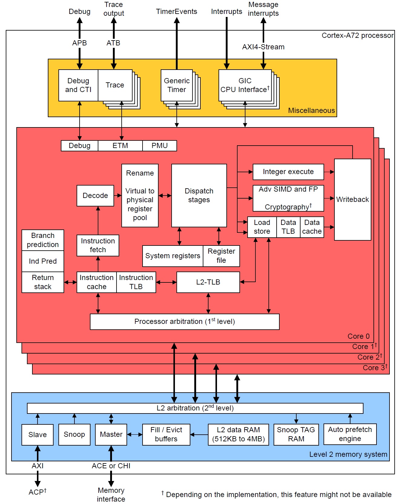
The Cortex-A72 allows speculative execution. Without speculation, a CPU must wait at each conditional program branch until the direction is decided and instruction fetch can proceed along the chosen branch. The Core-A72 processor predicts branch direction (speculates) and aggressively issues instructions along predicted branches. The Cortex-A72 branch predictor is also improved over ARM1176. (I’m still digging into details.) If a branch is mispredicted, speculative results are discarded. So, it’s important to have a good branch predictor.
The Cortex-A72 can perform a load operation and a store operation every cycle because it has separate load and store pipelines. The ARMv8-A instruction set architecture (ISA) allows arbitrary data alignment and access. However, the Cortex-A72 hardware penalizes load operations that cross a cache-line (64-byte) boundary and store operations that cross a 16-byte boundary. Programmers (and compilers) should keep that in mind when laying down data structures in memory.
Like all modern high-performance computers, the Cortex-A72 organizes physical memory into a hierarchy with the fastest/smallest memory (registers) near the arithmetic/logic unit (ALU) and the slowest/largest memory (RAM) far away and off-chip. The registers and RAM are connected to intervening levels of memory — the caches:
          Register          Fast, but small
             |
       Level 1 caches
             |
       Level 2 cache
             |
            RAM             Big, but slow
Data and instructions are read (and written) in efficient chunks making data and instructions available when needed by the registers and ALU. The chunks are called “cache lines.” Thanks to cache memory, programs run faster when they (re)use data that are close together in memory (i.e., occupy the same cache line) and are the most recently accessed. These notions are called “spatial locality” and “temporal locality.”
The following table is a quick summary of the level 1 and level 2 cache structures of the ARM1176 and Cortex-A72.
| Feature | ARM1176 | Cortex-A72 |
|---|---|---|
| L1 I-cache capacity | 16KB | 48KB |
| L1 I-cache organization | 4-way set associative, 32B line | 3-way set associative, 64B line |
| L1 D-cache capacity | 16KB | 32KB |
| L1 D-cache organization | 4-way set associative, 32B line | 2-way set associative, 64B line |
| L2 cache capacity | 128KB | 1MB |
| L2 cache organization | Shared, 8-way set associative, 64B line | Shared, 16-way set associative, 64B line |
Each core has an Instruction Cache (I-Cache) and Data Cache (D-Cache). The four cores share the Level 2 (L2) cache.
As you can see, the RPi4 (BCM2711) has larger caches and a bigger cache line size (64 bytes) than ARM11. RPi4 programs are more likely to find instructions and data in cache than earlier RPi models.
Contemporary processors have one or more memory management units (MMU) that break physical RAM into logical pages. This scheme is called “virtual memory.” The MMU translate logical program addresses (from loads, stores and instruction fetches) into physical RAM addresses. Address translation has its own memory hierarchy:
   Translation registers       Fast, but only a single mapping
             |
       Level 1 TLBs
             |
       Level 2 TLB
             |
            RAM                Big page tables, but slow
Page tables in RAM are maps that describe the layout of pages in the operating system and application programs. Translation lookaside buffers (TLB) are cache-like hardware structures that hold the most recently used (MRU) address translation information, i.e., where a logical page is located in physical memory. TLBs greatly speed up the translation process by keeping MRU page table information on-chip within the CPU.
Cortex-A72 has larger translation lookaside buffers (TLB) than ARM1176, as summarized in the table below. With larger TLBs, a program can touch more locations in memory without triggering a performance robbing page fault — an event which brings page translation information into the CPU from relatively slow RAM.
| Feature | ARM1176 | Cortex-A72 |
|---|---|---|
| D-MicroTLB capacity | 10 entries | 32 entries |
| D-MicroTLB organization | Fully assoc, 1 lookup/cycle | Fully assoc, 1 lookup/cycle |
| I-MicroTLB capacity | 10 entries | 48 entries |
| I-MicroTLB organization | Fully assoc, 1 lookup/cycle | Fully assoc, 1 lookup/cycle |
| L2 TLB capacity | 256 entries | 1024 entries |
| L2 TLB organization | Unified, 2-way set assoc | Unified, 4-way set assoc |
Each core has a Data Micro-TLB (D-MicroTLB), Instruction Micro-TLB (I-MicroTLB), and Level 2 (L2) TLB. (In ARM1176 terminology, the L2 TLB is called the “Main TLB”).
In summary, the RPi4’s BCM2711 processor is a powerhouse even though it won’t knock that gaming machine off your desktop. 🙂 If you’ve been waiting to dive into Raspberry Pi or to upgrade, please don’t hesitate any longer.
I’m getting the itch to play with RPi4’s hardware performance counters and post results. In the meantime, check out my summary of the ARM11 micro-architecture. If you would like to know more about performance measurement and events in ARM1176-based Raspberry Pi’s, please see my Performance Events for Linux (PERF) tutorial.
Also, I have uploaded all of my teaching notes about computer design, VLSI systems and computer architecture:
These resources should help students and teachers alike!
Copyright © 2020 Paul J. Drongowski
Pingback: ARM Cortex-A72 fetch and branch processing #ARM #RaspberryPi4 « Adafruit Industries – Makers, hackers, artists, designers and engineers!
Pingback: ARM Cortex-A72 fetch and branch processing #ARM #RaspberryPi4 - Piss 'N Shit