Please don’t forget my Performance Events for Linux tutorial and learn to make your own Raspberry Pi 4 (Broadcom BCM2711) performance measurements. The commands in the PERF tutorial apply to x86, AMD64 and other architectures, too.
There are a few surprises, too, such as earlier versions of code, etc.
The programs self-monitor, that is, they call perf_event_open() to configure, control and read the performance counters. perf_event_open() has many parameters, so I wrote helper functions assisting counter configuration, control and access. There are two flavors: architecture independent and Cortex-A72 specific. The architecture independent functions are defined in pe_assist.* and the A72-specific functions are defined in pe_cortex_a72.*. The architecture independent functions should work on x86, etc., too.
Aside from the two check-out tests, the rest of the source modules are workloads. These are the programs that I used to collect data for the articles about Cortex-A72 performance measurement, analysis and tuning. Feel free to bash away at everything!
Helper functions
As I mentioned above, I separated the helper functions into architecture independent and Cortex-A72 specific modules. The architecture independent helper functions handle Linux performance counter set-up, control and read back:
peInitialize(): Initialize/reset the helper module:
peMakeGroup(): Make a counter group
peAddLeader(): Add leader event to the group
peAddEvent(): Add an event to the group
peStartCounting(): Start the counter group
peStopCounting(): Stop the counter group
peResetCounters(): Reset the counters
peReadCount(): Read an event count
pePrintCount(): Print and event count
The interface is “lite” and uncomplicated. It’s just enough to get the job done. Sometimes during early days, there is a temptation to build the Taj Mahal. I prefer to build something simple and get experience before building up and out. This simple interface proved to be good enough.
perf_event_open() supports simple event counting and sampling. If you’re familiar with perf stat, you’ve already seen simple event counting, AKA counting mode. perf stat measures events across the entire run of an application program. Self-monitoring is similar except you insert measurement code into the application program around the critical code that you wish to measure. perf stat doesn’t require code modification or recompile, but it doesn’t let you focus on particular critical loops or whatever. Self-monitoring is a little bit more effort, but it allows focus.
The usage model is straightforward:
Initialize the module data structures.
Create a performance event group.
Add a leader event to the group.
Add other events (up to 6 events for Cortex-A72) to the group.
Start the counter group.
Execute the workload or critical inner loops.
Stop the counter group.
Read and print the event counts.
Since this sequence is a recurring pattern, I also wrote a few functions which target common types of measurements such as:
peMeasureInstructionEvents()
pePrintInstructionEvents()
peMeasureDataAccessEvents()
pePrintDataAccessEvents()
These functions configure the pre-defined “symbolic” events which the Linux kernel has preselected for the platform architecture. Thus, you should be able to use the pe_assist.* module on any Linux box.
The Cortex-A72 module, pe_cortex_a72.*, use “raw” event identifiers for configuration. The available events are defined in pe_cortex_a72.h and they are specific to ARM Cortex-A72. I rely mainly on the Cortex-A72 events because then I know exactly which A72 events I am measuring. The Cortex-A72 module calls the low-level helper functions and it exports only targeted measurement functions:
a72MeasureInstructionEvents()
a72PrintInstructionEvents()
a72MeasureDataAccessEvents()
a72PrintDataAccessEvents()
a72MeasureTlbEvents()
a72PrintTlbEvents()
Take a peek inside one of the test programs and you’ll see how to call the helper modules.
Internal design
perf_event_open() is the Swiss Army knife of performance counter configuration and control. On Linux, all counter-related operations go through this single kernel call.
perf_event_open() allows control of individual counters, of course. However, it also provides a way to control a group of counters. One can save additional trips in and out of the kernel through counter groups. Instead of making six calls to start six counters, one only needs to make one perf_event_open() call to start an entire group of six events.
A Cortex-A72 group consists of one to six event counters. Each group has a distinguished member: the leader event. You can start, stop and reset the entire group by referring to the leader. Because the group members usually share characteristics like the process (ID) to be measured, the CPU set, flags, etc., it makes sense to define all of these common properties for an entire group. This approach reduces the number of parameters to be passed around during configuration.
In keeping with the “lite” philosophy, the helper module keeps the common flags and such in a few variables and arrays. The group and leader definition functions establish group-wide values for the member events in the group. That’s all there is to it, so hack away! The “lite” approach was good enough 99% of the time, so you might not need to dip into the helper modules at all.
Today’s post characterizes read access time to three different levels of the Raspberry Pi 4 (Broadcom BCM2711) memory hierarchy. The ARM Cortex-A72 processor has a two level cache structure: Level 1 data (L1D) cache and unified Level 2 cache. There is one L1D cache per core and all four cores share the L2 cache. Primary memory is the third and final level beyond L2 cache.
The test program is a simple kernel (inner loop) that runs through a linked list, i.e., pointer chasing. Each linked list element is exactly one A72 cache line in size, 64 bytes. I have used pointer chasing on other non-ARM architectures (Alpha and AMD64 come to mind) and it’s a pretty simple and effective way to characterize memory access speed.
The trick is to adjust the number of linked elements so that the entire linked list fits entirely within the memory to be characterized. In order to facilitate run-to-run comparisons, there is an outer loop which repeatedly invokes list chasing, i.e., the entire list is walked multiple times per run.
There are two main run parameters:
The number of linked list elements (which determines the array size), and
The number of iterations (which is the number of times the full list is walked).
When the array is doubled, the number of iterations is cut in half. This keeps the number of individual pointer chase operations (approximately) constant across runs.
The following table summarizes the test run parameters and the memory level to be exercised by the each run:
Both Linux clock() time and Cortex-A72 performance counter events are measured.
In my first experiments, the linked list elements were laid down in a linear sequential fashion and in a simple ping-pong scheme. I quickly discovered that Cortex-A72’s aggressive data prefetch is too good and naive layout did not produce the expected number of L1D or L2 cache misses. A72 speculatively reads the next cache line beyond a miss. By the time execution would reach the list element beyond the current one (or the very next element), the needed destination element would be available in cache or in flight.
Ideally, we want to fool the memory prefetcher and hit only the intended memory level, taking the full read access penalty each time we chase a pointer. I rewrote array/list initialization to lay down the list elements at (pseudo-)random positions in the array. The Fisher-Yates (Knuth) shuffle algorithm got the job done. Once list element layout was randomized, the pointer chasing test began producing the expected number of reads and misses.
The following table summarizes each run by the number of retired instructions, CPU cycles, instructions per cycle (IPC) and execution time:
No surprise, access to L1D cache is best, L2 is second best and primary memory is worst. Access to L2 cache is about five times as long as L1D cache, in terms of CPU cycles. Access to primary memory is nearly 50 times longer than L1D cache. The effect on IPC is very significant.
Taking a look at the L1D performance event counts:
we see that pointer chasing correctly and independently exercises L1D cache according to design. The L1D cache capacity is 32KB. The particular 32KB run shown here has the shortest execution time of the 32KB runs and thus, is cherry-picked. As I’ve seen on other architectures, measurements get a bit “weird” near cache capacity. When a cache gets nearly full, “weird stuff” starts to happen and run statistics become inconsistent. The shortest run best shows the break between L1D and L2 access.
Finally, here are the L2 cache performance event counts.
As expected, we see a dramatic breakpoint at 1MB, which is the capacity of the unified L2 cache.
Bottom line, these performance measurements reinforce the importance of cache-friendly algorithms and data access patterns. Start with the best algorithms for your application, measure cache events and then tune for minimum misses. Data access should hit most frequently in the Level 1 data cache, then L2 cache. Primary memory is fifty times (!) more expensive than L1D cache and reads out to primary memory should be as infrequent as possible. Your mantra should be, “Bring it into cache, compute the heck out of the in-cache data, then write the final results back to memory, and move on.”
I’m in the midst of investigating a performance anomaly which seemingly pops up at random. I wrote a pointer chasing program to exercise and measure cache miss performance events. As part of the testing regimen, I run the program several times in a row and compare run time, event counts, etc. and look for inconsistencies.
The program is usually well-behaved/consistent and produces the expected result. For example, when the program is configured to always hit in the level 1 data (L1D) cache, the program measures just a few L1D misses and the run time is short. However, occasionally a run is slow and has a slew of L1D misses. What’s up?
My first thought was re-scheduling, that is, the pointer chasing program starts on one core and is moved by the OS to another core. The cache on the new core is cold and more misses occur. The Linux taskset command launches and pins a program to a core. In fancier language, it sets the CPU affinity for a (running) process. If we pin the program to a particular core, the cache should stay warm.
If you’re an old-timer and haven’t used taskset in a while, please be aware that a user must have CAP_SYS_NICE capability to change the affinity of a process. You can also set CAP_SYS_NICE capability for an application binary using the setcap utility:
sudo setcap 'cap_sys_nice=eip' <application>
You can check capabilities with getcap:
getcap <application>
The form of the capabilities string is in accordance with the cap_from_text call, so I recommend viewing its man page. The eip flags are case sensitive and specify the effective, inheritabe and permitted sets, respectively.
As to the performance anomoly, setting the CPU (core) affinity did not resolve the issue. Long runs and misses kept popping up. My next thought was “maybe CPU clock throttling?”
There’s quite a bit of on-line material about Raspberry Pi clock throttling and I won’t repeat all of it here. Suffice it to say, the RPi 4 firmware has a so-called CPU scaling governor that kicks in at high temperatures. The governor tries to keep the CPU temperature below 80℃ . Over-temperature occurs when the temperature rises above 85℃ . The governor adjusts (throttles) the CPU clock to achieve the configured operating temperature goals.
We do know that Raspberry Pi 4 can run hot. My RPi4 has heat sinks installed, but no case fan. Heat vents out the top of the Canakit plastic enclosure. The heat sinks are warm to the touch, not super hot, really. However, it’s not a bad idea to take the Pi’s temperature.
The following command displays the RPi’s temperature:
cat /sys/class/thermal/thermal_zone0/temp
Divide the result by 1000 to obtain the temperature in degrees Celsius. The next command displays the current frequency (kHz):
Divide the result by 1000 to obtain the frequency in MHz. This frequency is the Linux kernel’s requested frequency. The actual, possibly throttled frequency may be different.
The Pi’s vcgencmd command is even better! vcgencmd is the Swiss Army knife of system info utilities. The following command displays a list of vcgencmd subcommands:
vcgencmd commands
Here’s a few commands to get you started:
    vcgencmd measure_temp
    vcgencmd measure_clock arm
    vcgencmd measure_volts core
    vcgencmd get_throttled
You may run into permission issues with vcgencmd. I couldn’t tame the permissions and simply ran vcgencmd via sudo.
The get_throttled subcommand returns a bit mask. Here’s the magic decoder ring:
    Bit   Hex value  Meaning
    ----  ---------  -----------------------------------
    0     1          Under-voltage detected (< 4.64V)
    1     2          Arm frequency capped (temp > 80'C)
    2     4          Currently throttled
    3     8          Soft temperature limit active
    16    10000      Under-voltage has occurred
    17    20000      Arm frequency capping has occurred
    18    40000      Throttling has occurred
    19    80000      Soft temperature limit has occurred
If all of that isn’t enough, you can install and run cpufrequtils:
    sudo apt install cpufrequtils
    cpufreq-info
After running the workload and measuring both CPU clock and temperature, throttling did not appear to be a problem. My current conjecture has to do with Linux fixes for the Spectre security vulnerability. In short, Spectre is a class of vulnerabilities exploiting observable side-effects of the machine micro-architecture in order to set up clandestine information channels that leak confidential data. One way to supress data cache observables is to flush (clean) and invalidate the data caches during a context switch. If the data cache is invalidated, cache misses and program run time will go up. Stay tuned.
Even though I haven’t found the source of the performance anomoly, I welcomed the chance to learn about vcgencmd, etc. Off to investigate Linux hardware cache flushing…
Back on the old day job, I developed and tested software and hardware for program profiling. Testing may sound like drudge-work, but there are ways to make things fun!
Two questions arise while testing a profiling infrastructure — software plus hardware:
Does the hardware accurately count (or sample) performance events for a given specific workload?
Does the software accurately display the counts or samples?
Clearly, ya need working hardware before you can build working software.
Testing requires a solid, known-good (KG) baseline in order to decide if new test results are correct. Here’s one way to get a KG baseline — a combination of static analysis and measurement:
Static analysis: Analyze the post-compilation machine code and predict the expected number of instruction retires, cache reads, misses, etc.
Measurement: Run the code and count performance events.
Validation: Compare the measured results against the predicted results.
Thereafter, one can compare new measurements taken from the system under test (SUT) and compare against both predicted results and baseline measured results.
Applying this method to performance counter counting mode is straightforward. You might get a little “hair” in the counts due to run-to-run variability, however, the results should be well-within a small measurement error. Performance counter sampling mode is more difficult to assess and one must be sure to collect a statistically significant number of samples within critical workload code in order to have confidence in a result.
One way to make testing fun is to make it a game. I wrotekernel programs that exercised specific hardware events and analyzed the inner test loops. You could call these programs “test kernels.” The kernels are pathologically bad (or good!) code which triggers a large number of specific performance events. It’s kind of a game to write such bad code…
The expected number of performance events is predicted through machine code level complexity analysis known as program “microanalysis.” For example, the inner loops of matrix multiplication are examined and, knowing the matrix sizes, the number of retired instructions, cache reads, branches, etc. are computed in closed form, e.g.,
This formula is the closed form expression for the retired instruction count within the textbook matrix multiplication kernel. The microanalysis approach worked successfully on Alpha, Itanium, x86, x64 and (now) ARM. [That’s a short list of machines that I’ve worked on. 🙂 ]
With that background in mind, let’s write a program kernel to deliberately cause branch mispredictions and measure branch mispredict events.
The ARM Cortex-A72 core predicts conditional branch direction in order to aggressively prefetch and dispatch instructions along an anticipated program path before the actual branch direction is known. A branch mispredict event occurs when the core detects a mistaken prediction. Micro-ops on the wrong path must be discarded and the front-end must be steered down the correct program path. The Cortex-A72 mispredict penalty is 15 cycles.
What we need is a program condition that consistently fools the Cortex-A72 branch prediction hardware. Branch predictors try to remember a program’s tendency to take or not take a branch and the predictors are fairly sensitive; even a 49%/51% split between taken and not taken has a beneficial effect on performance. So, we need a program condition which has 50%/50% split with a random pattern of taken and not taken direction.
Here’s the overall approach. We fill a large array with a random pattern of ‘0’ and ‘1’ characters. Then, we walk through the array and count the number of ‘1’ characters. The function initialize_test_array() fills the array with a (pseudo-)random pattern of ones and zeroes:
void initialize_test_array(int size, char* array,
               int always_one, int always_zero)
{
    register char* r = array ;
    int s ;
    for (s = size ; s > 0 ; s--) {
        if (always_one) {
            *r++ = '1' ;
        } else if (always_zero) {
            *r++ = '0' ;
        } else {
            *r++ = ((rand() & 0x1) ? '1' : '0') ;
        }
    }
}
The function has options to fill the array with all ones or all zeroes in case you want to see what happens when the inner conditional branch is well-predicted. BTW, I made the array 20,000,000 characters long. The size is not especially important other than the desire to have a modestly long run time.
The function below, test_loop(), contains the inner condition itself:
int test_loop(int size, char* array)
{
    register int count = 0 ;
    register char* r = array ;
    int s ;
    for (s = size ; s > 0 ; s--) {
        if (*r++ == '1') count++ ;    // Should mispredict!
    }     return( count ) ;
}
The C compiler translates the test for ‘1’ to a conditional branch instruction. Given an array with random ‘0’ and ‘1’ characters, we should be able to fool the hardware branch predictor. Please note that the compiler generates a conditional branch for the array/loop termination condition, s > 0. This conditional branch should be almost always predicted correctly.
The function run_the_test() runs the test loop:
void run_the_test(int iteration_count, int array_size, char* array)
{
  register int rarray_size = array_size ;
  register char* rarray = array ;
  int i ;
  for (i = iteration_count ; i-- ; ) {
      test_loop(array_size, array) ;
  }
}
It calls test_loop() many times as determined by iteration_count. Redundant iterations aren’t strictly necessary when taking measurements in counting mode. They are needed, however, in sampling mode in order to collect a statistically significant number of performance event samples. I set the iteration count to 200 — enough to get a reasonable run time when sampling.
The test driver code initializes the branch condition array, configures the ARM Cortex-A72 performance counters, starts the counters, runs the test loop, stops the counters and prints the performance event counts:
The four counter configuration, control and display functions are part of a small utility module that I wrote. I will explain the utility module in a future post and will publish the code, too.
Finally, here are the measurements when scanning an array holding a random pattern of ‘0’ and ‘1’ characters:
Please recall that there are two conditional branches in the inner test loop: a conditional branch to detect ‘1’ characters and a conditional branch to check the array/loop termination condition. The loop check should be predicted correctly almost all the time, accounting for 50% of the total number of correctly predicted branches. The character test, however, should be incorrectly predicted 50% of the time. It’s like guessing coin flips — you’ll be right half the time on average. Overall, 25% of branch predictions should be incorrect, and yes, the measured branch mispredict ratio is 0.250 or 25%.
The number of speculated instructions is also very interesting. Cortex-A72 speculated twice as many ARMv8 instructions as it retired. Over half of the speculated instructions did not complete architecturally and were discarded. That’s what happens when a conditional branch is grossly mispredicted!
In my discussion about instructions per cycle as a performance metric, I compared the textbook implementation of matrix multiplication against the loop next interchange version. The textbook program ran slower (28.6 seconds) than the interchange version (19.6 seconds). The interchange program executes 2.053 instructions per cycle (IPC) while the textbook version has a less than stunning 0.909 IPC.
Let’s see why this is the case.
Like many other array-oriented scientific computations, matrix multiplication is memory bandwidth limited. Matrix multiplication has two incoming data streams — one stream from each of the two operand matrices. There is one outgoing data stream for the matrix product. Thanks to data dependency, the incoming streams are more important than the outgoing matrix product stream. Thus, anything that we can do to speed up the flow of the incoming data streams will improve program performance.
Matrix multiplication is one of the most studied examples due to its simplicity, wide-applicability and familiar mathematics. So, nothing in this note should be much of a surprise! Let’s pretend, for a moment, that we don’t know the final outcome to our analysis.
I measured retired instructions, CPU cycles and level 1 data (L1D) cache and level 2 (L2) cache read events:
There is one big take-away here. The textbook program misses in the data cache far more often than interchange. The textbook L1D cache miss ratio is 0.073 (7.3%) while the interchange cache miss ratio is 0.001 (0.1%). As a consequence, the textbook program reads the slower level 2 (L2) cache more often to find necessary data.
If you noticed slightly different counts for the same event, good eye! The counts are from different runs. It’s normal to have small variations from run to run due to measurement error, unintended interference from system interrupts, etc. Results are largely consistent across runs.
The behavioral differences come down to the memory access pattern in each program. In C language, two dimensional arrays are arranged in row-major order. The textbook program touches one operand matrix in row-major order and touches the other operand matrix in column-major order. The interchange program touches both operand arrays in row-major order. Thanks to row-major order’s sequential memory access, the interchange program finds its data in level 1 data (L1D) cache more often than the textbook implementation.
There is another micro-architecture aspect to this situation, too. Here are the performance event counts for translation look-aside buffer (TLB) behavior:
    Event                          Textbook     Interchange
    -----------------------  --------------  --------------
    Retired instructions     38,227,830,517  60,210,830,503
    L1 D-cache reads         15,070,845,178  19,094,937,273
    L1 DTLB miss              1,001,149,440          17,556
    L1 DTLB miss LD           1,000,143,621          10,854
    L1 DTLB miss ST               1,005,819           6,702
Due to the chosen matrix dimensions, the textbook program makes long strides through one of the operand matrices, again, due to the column-major order data access pattern. The stride is big enough to touch different memory pages, thereby causing level 1 data TLB (DTLB) misses. The textbook program has a 0.066 (6.6%) DTLB miss ratio. The miss ratio is near zero for the interchange version.
I hope this discussion motivates the importance of cache- and TLB-friendly algorithms and code. Please see the following articles if you need to brush up on ARM Cortex-A72 micro-architecture and performance events:
Here is a list of the ARM Cortex-A72 performance events that are most useful for measuring memory access (load, store and fetch) behavior. Please see the ARM Cortex-A72 MPCore Processor Technical Reference Manual (TRM) for the complete list of performance events.
you’re probably wondering, “How I do I reduce all of this to practice on Raspberry Pi 4?”
Program performance tuning is experimental and is measurement-based. Our goal is to reduce program execution time by efficiently exploiting the underlying machine micro-architecture. Tuning follows a systematic, multi-step process:
Initial design and code.
Run and measure execution time and performance events.
Analyze measurements.
Make a hypothesis about performance bottlenecks.
Change the code.
Go to step 2 until you’re satisfied.
“Satisfied” is a bit subjective, but generally means “produces a result within a defined time constraint”, “achieves the desired frame rate,” or some other time-related design requirement.
You will need performance measurement tools and techniques. This is where hardware performance events come into play. Raspberry Pi OS is Linux, and fortunately, Linux has a mature performance measurement infrastructure. Performance Events for Linux, often called “PERF,” is the best way to get started. I’ve written extensively about PERF including my three part PERF tutorial:
The PERF tutorial illustrates performance measurement and tuning on Raspberry Pi models 1, 2 and 3. The mechanics of running PERF are the same on Raspberry Pi 4. Please see my other articles about Cortex-A72 performance tuning:
Lately, I have been experimenting with program performance self-monitoring using the Linux perf_event_open() system call. Stay tuned for more details and code. For the moment, I’m going to focus on ARM Cortex-A72 performance events — good enough to help you apply techniques and commands in the PERF tutorial.
Cortex-A72 performance events
A performance event is the occurrence of a micro-architectural condition. The simplest example events are retired instructions and processor (CPU) cycles. A retired instruction event occurs every time an instruction successfully completes (architectural) execution. A processor cycle event occurs every processor clock tick.
Each Cortex-A72 core has six performance counter registers. Using a tool like PERF, a performance event is assigned to each register. Yes, you can measure up to six performance events simultaneously, i.e., in a single experimental execution run. [More events can be measured via counter multiplexing, but I’m keeping things simple here.] The trick is to choose and configure the performance events that help you test your performance tuning hypothesis.
The ARM Cortex-A72 performance events are listed in the ARM Cortex-A72 Technical Reference Manual (TRM) available at the ARM corporate web site. The list is rather long and not all of the events are particularly relevant for application programmers. Thus, I won’t list them all here. There are several major event categories:
Instructions and cycles
Level 1 instruction (L1I) cache events
Level 1 data (L1D) cache events
Level 2 (L2) cache events
Level 1 instruction TLB (L1 ITLB) events
Level 1 data TLB (L1 DTLB) events
Branches and mispredicted branches
Bus and primary memory access
Memory barriers (speculative)
Instruction mix (speculative)
Exceptions taken
System register access
These are my own categories and should give you a rough impression about the kinds of micro-architectural events you can measure on Raspberry Pi 4. I listed the categories from highest to lowest priority placing the most relevant and generally useful event categories near the top of the list.
Each Coretex-A72 performance event type is assigned an event number. The event number identifies the event to measurement tools and to the event counting hardware.
Time and instruction events
Processor/CPU cycles and retired instructions are the true all-rounders.
Processor cycles are a good proxy for actual execution time. Sure, you can measure wall-clock or CPU execution time using the Linux time command or system calls like gettimeofday(), time(), clock() or clock_gettime(). The CPU cycle event lets us measure time using a performance counter register. The cycle count tells us approximately how much CPU time was consumed by the program under test.
As mentioned earlier, the retired instruction event counts the number of successfully (architecturally) completed instructions. Given a specific data set, every program has a specific amount of work to be accomplished. Particularly in the case of a single-threaded program, the program executes the same instructions for the same given data set, every time. Thus, the retired instruction count is a measure of work accomplished and should be (roughly) the same every experimental run, assuming the same data set and no outside interference. (You shouldn’t run other applications while testing. Control the test environment!)
    Number  Mnemonic      Name
    ------  ------------  ------------------------------------
    0x08    INST_RETIRED  Instruction architecturally executed
    0x11    CPU_CYCLES    Cycle
    0x1B    INST_SPEC     Operation speculatively executed
Instructions per cycle (IPC)
Two basic performance tuning goals are:
Reduce the number of processor cycles, and
Reduce the number of retired instructions.
Reducing the number of processor cycles should reduce the overall execution time. That assumes, of course, that overall execution time is not dominated by input/output, page faults, human wait (interaction) time, or some other major factor!
Reducing the number of retired instructions should reduce the amount of work performed by the program. Optimizing compilers work hard to reduce the number of instructions in tight inner loops. In terms of conventional wisdom, the fastest instruction is an instruction which is never executed in the first place.
Practically, however, one program can execute more instructions and achieve a shorter execution time than another program (assuming the same data set and functionality, of course). How can this be? It comes down to a few fundamental factors:
Read and use data from fast cache memory.
Reducing reads (writes) from (to) slow primary memory.
Execute computations concurrently.
Overlap execution with read and write operations.
Short answer, it comes down to exploiting instruction-level parallelism (ILP), temporal data locality and spatial data locality.
Instructions per cycle(IPC) is one simple measure that tells us how we are doing overall. IPC is easy to measure and compute: Count the number of retired instructions, count the number of processor cycles, and divide:
INST_RETIRED / CPU_CYCLES
The IPC ratio indicates the amount of useful work done during each processor cycle and we want to maximize it.
Goal IPC is very much application dependent. For a given critical inner loop, one might ask, “How many concurrent operations (computations, reads, writes) can Cortex-A72 perform assuming the data are cache-resident?” If IPC is significantly less than one, it’s probably time to tune. In scientific code with a mix of integer and floating point operations, an IPC of 2 is a good starting goal.
The speculated instruction event count is the number of ARMv8-A issued speculatively during program execution. Ideally, branch predictions are always correct and every speculatively issued instruction eventually retires. Speculatively issued instructions on a wrong path consume execution resources just like correct path instructions that retire. Unfortunately, wrong path results are discarded, thereby wasting any resources which they consumed. Fewer wrong-path instructions produces less waste, that is, fewer wrong-path instructions start execution, consume resources, and are discarded.
The ratio of speculated instructions to retired instructions:
INST_RETIRED / INST_SPEC
indicates how often speculated instructions resolved into retirement. Best case, this ratio is one — all speculated instructions eventually retired (i.e., few execution resources are wasted).
Example: Matrix multiplication
Matrix multiplication is the classic example of performance tuning for micro-architecture. Mathematics specifies the end result — the matrix product. Algorithmically, however, there are two ways to compute the matrix product:
Textbook algorithm and code: Straightforward implementation of the mathematics.
Loop nest interchange algorithm and code: Cache-friendly implementation which exploits temporal and spatial locality.
I ran both the textbook and loop nest interchange programs on Raspberry Pi 4. The textbook code took 28.6 seconds and, as expected, the interchange code took more time, 19.6 seconds. Here are the raw event counts:
    Event                    Textbook        Interchange
    -----------------------  --------------  --------------
    Retired instructions     38,227,831,497  60,210,830,503
    CPU cycles               42,041,568,760  29,332,934,027
    Instructions per cycle   0.909           2.053
The textbook program executed less than one instruction per processor cycle, 0.909 IPC. The textbook code underperforms with respect to the availability of Cortex-A72 execution units (two integer, two FP units) and the opportunity to overlap computation with memory access. The interchange program achieves a respectable 2.053 instructions per cycle. The interchange version consumes far fewer processor cycles than the textbook version.
Just for grins, multiply the CPU cycle counts by the Raspberry Pi 4 clock period (the inverse of the 1.5GHz clock frequency). You get approximately the measured clock() CPU times: 28.028 seconds versus 28.6 actual and 19.555 seconds vs. 19.6 seconds actual.
Here are the raw event counts for retired and speculated instructions:
The interchange version has a near ideal retired to speculated instruction ratio (0.999). The textbook slightly underperforms with nearly 8 million speculated instructions started and abandoned.
The programs are written in C and compiled with the -O0 optimization level. Try -O3. The results may further surprise you. 🙂
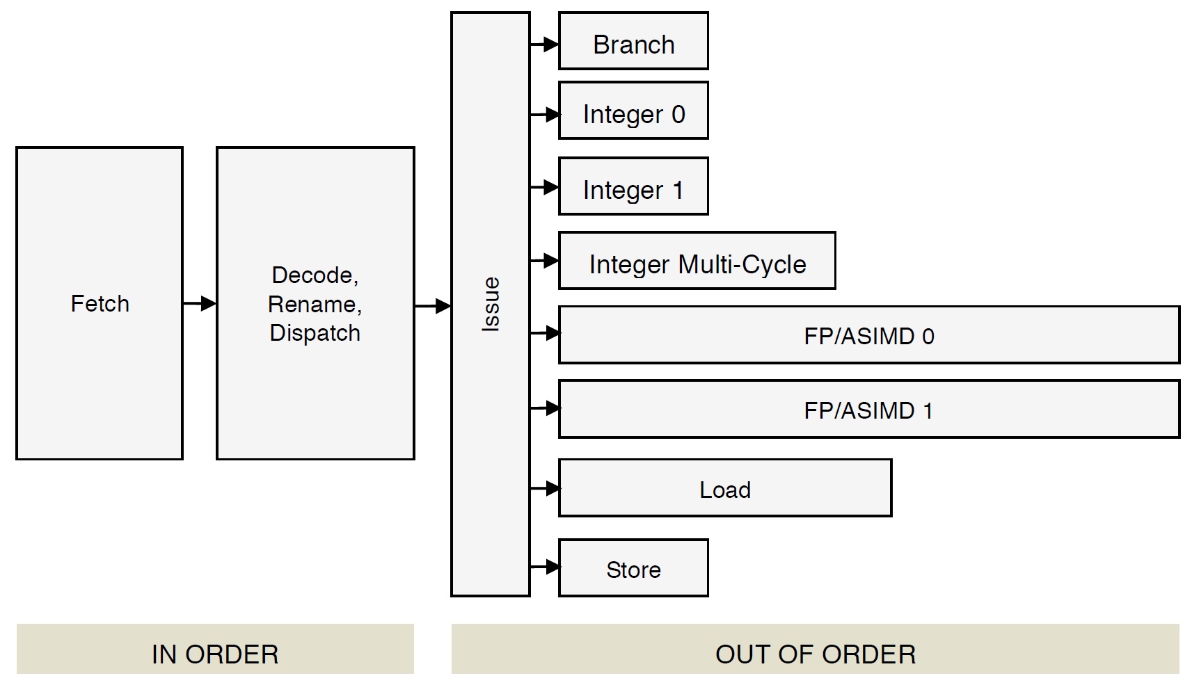
The Cortex-A72 front-end puts micro-ops into per-pipe issue queues which, in turn, feed the execution units. There are eight issue queues. The queues have eight entries each except the branch queue, which has ten entries (66 queue entries total like the old Cortex-A57). The queues provide rate-balancing between the core front-end (i.e., the instruction/micro-op stream) and the execution units. The queues allow greater parallelism between units, too, letting each pipeline run at its own independent single- or multi-cycle speed.
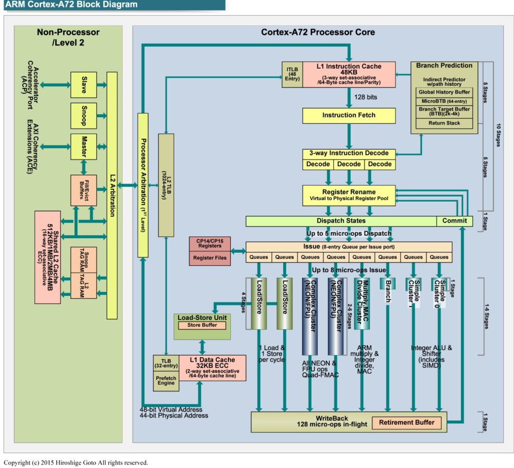
ARM Cortex-A72 micro-architecture (Source: Hiroshige Goto)
The branch and integer pipes are very fast, each pipe executing a micro-op in a single processor cycle. The integer pipelines have multiple, zero-cycle forwarding datapaths. These paths, sometimes called “by-passes,” send intermediate results directly to stages (computations) needing the result right darned now without writing the result into the rename register file first.
The integer multi-cycle pipe handles integer micro-ops which require 2 or more processor cycles for execution. Shift operations are relatively fast: 2+ cycles. Integer multiplication has a 3 to 5 cycle latency. Integer divide is relatively slow taking anywhere from 4 to 20 cycles. Multiplication can be accelerated through dedicated combinational logic; division is sequential by nature and requires many steps.
The FP (floating point) and ASIMD (Advanced Single Instruction Multiple Data) units perform floating point and SIMD computations. Both units are generalist and perform commonly occurring FP operations: FP ADD, SUB, MUL, NEG, ABS, MAX, MIN, etc. Execution latency varies from 3 to 4 cycles for these basic operations. The FP pipes support late forwarding of FP MUL products to FP multiply-accumulate micro-ops, letting FP multiply-accumulate complete in 6 cycles.
Each FP unit is a specialist, too:
FP/ASIMD 0: FP CONVERT, ROUND, DIV, CRYPTO
FP/ASIMD 1: FP COMPARE, SQRT
FP divide and square root operations are performed using iterative algorithms. Only one FP DIV or SQRT operation at a time may execute in a pipe. Latencies are long: 6 to 18 cycles for DIV and 6 to 32 cycles for SQRT, depending upon FP datatype.
Please see the ARM Cortex-A72 Software Optimization Guide for detailed instruction timing, pipe assignment and ASIMD operation.
Load and store micro-ops are executed by the load and store units. The load and store units are mutually independent. One load and one store micro-op can execute each processor cycle. (Load and store are discussed below.) Load and store micro-ops issue speculatively. Under speculative execution, a load or store may reside on a correctly predicted branch path (the correct path) or an incorrectly predicted branch path (the wrong path). Loads, stores and associated data on a wrong path must be discarded. Store operations are buffered (wait) until they are determined to be on the correct path and are committed architecturally to primary memory.
Memory hierarchy
As I mentioned in my Cortex-A72 overview, the Raspberry Pi 4 (Broadcom BCM2711) has a four level memory hierarchy:
          Register          Fast, but small
              |
        Level 1 caches
              |
        Level 2 cache
              |
             RAM             Big, but slow
The RPi4 has four A72 cores. Each core has a register file and level 1 instruction and data caches. The four cores share a single unified level 2 cache and primary memory (RAM).
The register file is the fastest, but has the smallest capacity. Registers are read or written in a single processor cycle. RAM has the most capacity, but is relatively slow. RPi4 primary memory is LPDDR4-3200 SDRAM:
The following table summarizes Cortex-A72 cache characteristics:
L1I cache capacity
48KB
L1I cache organization
Per-core, 3-way set associative, 64B line
L1D cache capacity
32KB
L1D cache organization
Per-core, 2-way set associative, 64B line
L2 cache capacity
1MB
L2 cache organization
Shared, 16-way set associative, 64B line
Data accesses are handled by the Level 1 Data (L1D) cache. Instruction fetches are handled by the Level 1 Instruction (L1I) cache. The Level 2 (L2) cache is unified, handling both data and instructions. The Raspberry Pi BCM2711 ARM Peripherals manual states the following caveat with respect to the L2 cache:
BCM2711 provides a 1MB system L2 cache, which is used primarily by the GPU. Accesses to memory are routed either via or around the L2 cache depending on the address range being used.
Thus, application programs should not expect to receive a performance assist from the L2 cache! The VideoCode GPU accesses L2 cache through the Cortex-A72 ACP/AXI interface.
The L1D cache load-to-use latency is 4 cycles when the load hits in the L1D cache. The Level 2 (L2) cache load-to-use latency is 9 cycles when the load hits in the L2 cache.
A read access (e.g., a data load or instruction fetch) first tries the appropriate level 1 cache (Load: L1D cache, Fetch: L1I cache). If it finds the requested item in the level 1 cache — a hit — the item is sent to either the rename registers (for loads) or the instruction decoder (for fetches). Load data may also be sent through a bypass to an execution stage (micro-op) awaiting the incoming data.
If the read access misses the level 1 cache, the request is sent (optionally) to the unified L2 cache. If the requested item is found in L2 cache, the cache line containing the item is written into the level 1 cache, thereby replacing one of the existing lines. This operation is called a “refill.” If the line to be replaced is dirty (modified), then the old value is evicted and is written to primary memory. The requested item is selected from the incoming cache line and is routed to the appropriate destination (i.e., functional unit or instruction decoder).
If the read access misses (or optionally, bypasses) the L2 cache, the 64 byte line containing the item is read from primary memory. The incoming line is written to the level 1 cache (a refill) and (optionally) the L2 cache. Again, dirty lines are evicted.
Instruction and data bytes are read, written and transferred in 64-byte chunks (lines). This is true even if a load instruction requests a single byte from memory. Application programs should strive to use each entire cache line completely before moving on to the next line. Programs that exploit spatial and temporal locality perform better. Programmers need to pay careful attention to algorithm selection, data structure/layout and memory access patterns in order to make good, efficient use of data caching.
The description of Cortex-A72 cache operation above is simplified. Consider, for example, memory transaction types. Memory attributes within the Memory Management Unit (MMU) and page tables determine memory transaction types for each memory region:
Write-Back Read-Write-Allocate
Write-Back No-Allocate
Write-Through
Non-cacheable
Device
Memory transaction type affects cache behavior.
Write-Back Read-Write-Allocate is the most common and highest performing memory type. Incoming lines are written to the L1D cache and the read (or write) completes from the L1D cache. A store that hits a Write-Back cache line does not update main memory.
Write-Back No-Allocate does not write an incoming line to L1D cache. This prevents cache pollution when accessing large, one-time use data structures.
Non-cacheable memory bypasses both the level 1 caches and L2 cache. Requests go directly to primary memory. The Cortex-A72 treats Write-Through memory as Non-cacheable.
Instruction fetch (more details)
Instruction fetches are speculative and there is no guarantee that fetched instructions are executed. Instructions are aggressively prefetched pursuing either sequential execution flow or branch targets based on path prediction.
The L1I cache is fed by three fill buffers that hold instructions from either the unified L2 cache or primary memory. The fill buffers are non-blocking. A line may remain in a fill buffer until it is transferred to the L1I cache or discarded. Primary memory regions may be marked as non-cacheable regions or the L1I cache may be disabled, and incoming lines are not written to the L1I cache. A line is not committed to the L1I cache unless it is demanded by a fetch. The hardware also has an L2 instruction prefetcher.
Cortex-A72 treats the preload instruction cache instruction (PLDI) as a NOP.
Memory Management Unit
The Memory Management Unit (MMU) performs virtual to physical address translation and enforces secure, restricted access to memory regions. As to security, suffice it to say that the MMU restricts access by Address Space Identifier (ASID) and Virtual Machine Identifier (VMID). These concerns are addressed by the operating system and are generally transparent to application programmers. [And I won’t be dealing with access control here.]
Address type
AArch64
AArch32
Virtual address (VA)
48 bits
32 bits
Physical address (PA)
44 bits
40 bits
The Cortex-A72 hardware supports 4KB, 64KB and 1MB page sizes. The Raspberry Pi Operating System (formerly known as “Raspbian”) organizes primary memory into 4KByte pages. [Huge pages must be enabled in the kernel and I will assume that it’s 4KB all the way on RPi4.] The operating system maintains page tables that specify the physical location of application program pages (both instructions and data).
Application programs use virtual addresses to identify instructions and data items. Conceivably, hardware could use memory-resident page tables to map a virtual address to its corresponding physical address. This approach is way too slow to be practical. Better, the Cortex-A72 maintains page (address) mapping information in a multi-level, hierarchical memory system:
       Level 1 TLB          Fast, but small
            |
       Level 2 TLB
            |
           RAM              Big page tables, but slow
The TLB structure is separate from the register/cache/memory hierarchy and it operates independently. The organizing principle is the same — most recent and frequently used mappings reside in fast memory and big page tables reside in slow primary memory.
“TLB” is the acronym for “translation lookaside buffer.” A TLB is an array where each entry describes the mapping from a virtual page to a physical page. Internal operation of a TLB is similar to a data cache. The following table summarizes Cortex-A72 TLB characteristics:
L1I TLB capacity
48 entries
L1I TLB organization
Fully associative
L1D TLB capacity
32 entries
L1D TLB organization
Fully associative
L2 TLB capacity
1024 entries
L2 TLB organization
4-way set associative
The L1I and L2D TLBs support 4KB, 64KB, and 1MB page sizes. The L2 TLB supports 4KB, 64KB, 1MB and 16MB page sizes. (Also, 2MB and 1GB using AArch32 long descriptor format translation.) Alas, Raspberry Pi OS uses 4KB pages.
TLB operation is similar to caching. Address translation is first tried in the L1I TLB (fetches) or L1D TLB (loads and stores). If the translation information is found (a hit), the physical address is returned in one cycle. Access permission is checked at the same time.
If translation misses in a level 1 TLB, address translation is attempted in the main L2 TLB. If the translation information is found, the physical address is returned (after one or more cycles).
If translation misses in the L2 TLB, the MMU performs a hardware translation table walk. (Page tables have a fairly complicated structure which is beyond the scope of this discussion.) Because page tables reside in slow primary memory, a hardware translation table walk takes a relatively long time to complete with respect to an L2 TLB look-up.
If the required page is not in memory and is on the RPi OS swap device, the operating system reads the page into primary memory before attempting re-translation. These exceptions, page faults, are the slowest of all and they should be avoided like the plague.
Once again, program performance depends up good temporal and spatial locality, albeit locality at the page level. An application program can touch as many as 32 different data pages without triggering an L1D TLB refill:
32 L1D TLB entries * 4 KBytes/page = 128 KByte data working set
This is a modest-sized working set of pages, and like cache line strategy, a program should make maximal, efficient use of a page working set before demanding new page translation information from the L2 TLB. The L2 TLB supports a larger combined data/instruction working set:
1024 L2 TLB entries * 4 KBytes/page = 4 MByte total working set
The L2 TLB footprint (working set size) is larger. However, the L1D TLB and the L1I TLB compete for page translation entries in the unified L2 TLB.
As to data-page utilization, data structure layout and access pattern come into play once again. A program should work as much as possible within the current working set before moving to pages outside the current set. Random access within a big heap pays a penalty when heap items are distributed across many pages (i.e., when the working set exceeds 32 pages).
With respect to L1I TLB utilization strategy, frequently executed, related code should reside within the same page or just a few pages. Related code which is spread across many pages (i.e., a large instruction working set) will jump between pages and possibly cause L1I TLB or L2 TLB refills.
The above description of the translation process is simplified. For example, access is checked against page permissions, etc. and violations are reported after aborting offending translation and instruction. I tried to focus mainly on performance-related concerns of interest to application programmers.
Load and store operations
After absorbing all of that, let’s pick up a few additional odds and ends about load and store operations.
Cortex-A72 memory operations are weakly ordered. They may be performed out-of-order as long as data dependencies are honored. Due to the weak ordering, explicit synchronization barriers are needed in circumstance where strong ordering is required. There are four kinds of barriers:
Instruction Synchronization Barrier (ISB)
Data Synchronization Barrier (DSB)
Data Memory Barrier (DMB)
Load-Acquire (LDAR) and Store-Release (STLR)
Please see the Programmer’s Guide for ARMv8-A for further details.
More generally important to application programmers is data alignment. Naturally aligned data is accessed faster than unaligned data, especially unaligned data items that cross cache line boundaries. The following table summarizes alignment requirements:
Source: Programmer’s Guide for ARMv8-A
Load operations should not cross 64-byte, cache line boundaries. Store operations should not cross 16-byte boundaries.
As a general program design principle, computations proceed as fast as data items can stream from primary memory, and secondarily, as fast as results can stream back to primary memory. Data prefetching increases the speed of incoming data stream(s). The programmer or compiler should schedule load operations further ahead of instructions which consume the incoming data item. Ideally, other independent instructions are scheduled and executed ahead of the consuming load thereby overlapping useful computation with load latency (4 cycles from the L1D cache at a minimum).
A program may signal the need for a data item through an explicit prefetch instruction. The A72 supports three instruction prefetch hint instructions: PLD, PLDW, and PRFM. These are only hints and may be ignored. The PLD and PLDW instructions allocate a line in the Level 1 Data cache. Prefetch from Memory (PRFM) hints that data from a specific address will soon be needed. If accepted, these hints can bring in a data item (cache line) before it is required.
Programmers may further manage data cache contents via non-temporal load and store instructions (LDNP and STNP). These instructions hint that caching is not useful for data at an address, thereby preventing unnecessary cache pollution. Non-temporal load and store instructions may require explicit load barriers. (See the Programmer’s Guide for ARMv8-A for more details.)
The Cortex-A72 hardware has a load-side prefetcher which dynamically analyzes memory access patterns. Based on its analysis, the load-side prefetcher brings data into either the L1D cache, the L2 cache, or both. The hardware also has a store-side prefetcher which brings data into the L2 cache.
Outgoing data streams benefit from write combining which merges data from multiple store operations into a single memory write access.
Outstanding read and write requests (i.e., pending requests to primary memory) wait in the Fill/Eviction Queue (FEQ). The Cortex-A72 has a configurable FEQ: 20, 24, or 28 entries. The A72 write issuing capability is 16, that is, up to 16 writes may be outstanding at any time. The read issuing capability is 19, 23, or 27 depending upon FEQ configuration (capacity). L2 prefetch is throttled based on the FEQ occupancy count. [Extra credit: What is the specific Raspberry Pi 4 FEQ configuration and occupancy threshold?]
One important simplification in the cache discussion is cache coherency. Most application programmers needn’t worry about cache coherency. However, if you are writing a program with multiple, co-operating threads that actively share memory locations or regions, you should MOESI over to the ARM Cortex-A72 Technical Reference Manual (TRM) and read up on the details. The A72 Snoop Control Unit (SCU) uses a hybrid protocol (MESI+MOESI) to maintain coherency between the per-core L1 data caches (MESI) and the common L2 cache (MOESI). “MESI” and “MOESI” refer to the coherency status of each cache line:
Modified (M)
Owned (O)
Exclusive (E)
Shared (S)
Invalid (I)
The BCM2711 employs an Advanced Microcontroller Bus Architecture (AMBA) Advanced xExtensible Interface (AXI) bus interface. Broadcom does not specify if either AXI Coherency Extensions (ACE) or the Coherency Hub Interface (CHI) are supported. (Man, these acronyms stack up!) Since ACE and CHI are intended for SMP processor clusters (e.g., big.LITTLE) these features may have been left out or disabled.
If you do care about cache coherency, please be aware that load data may be sourced from a remote L1D cache as well as the shared L2 cache or primary memory.
Sources
Before closing, I want to offer a few words about my sources. My primary resources are:
ARM Cortex-A72 Technical Reference Manual (TRM)
ARM Cortex-A72 Software Optimization Guide
ARM Programmer’s Guide for ARMv8-A
BCM2711 ARM Peripherals
These resources are authoritative. I also relied upon ARM’s own briefings and presentations about Cortex-A72 as found on the Web. I tried to verify Web sources and briefings against the written TRM and programmer guides.
In closing
Hopefully, my write-ups will help developers tune their programs for ARM Cortex-A72. If you’re just getting started with performance tuning, I would first concentrate on cache- and page-friendly algorithms, data structures and access patterns. Fill buffers, FEQ, memory ordering, and memory transaction types are esoteric subjects for most application programmers.
Want to learn more about Raspberry Pi 4 (Cortex-A72 / Broadcom BCM2711) performance tuning? Please read:
Let’s take a closer look at instruction fetch, decode and dispatch in the Cortex-A72 micro-architecture. These are the “front-end” stages of the core pipeline. The “back-end” of the pipeline consists of the register file(s), execution units and retirement (reorder) buffer. Branch prediction is frequently associated with the front-end since it directly affects instruction fetch.
The Cortex-A72 pipeline has 15 stages. [On-line sources disagree on the length; some sources claim 14 stages.] The front-end stages are:
Fetch (5 stages)
Decode (3 stages)
Rename (1 stage)
Dispatch (2 stages)
The back-end pipeline stages are:
Execute (1 to 6 stages depending upon unit)
Write-back/retirement (2 stages)
Each execution unit has its own pipe:
Integer 0 (1 stage/cycle)
Integer 1 (1 stage/cycle)
Integer multi-cycle (4 to 12 cycles)
FP/ASIMD 0 (6 to 18 cycles)
FP/ASIMD 1 (6 to 32 cycles)
Load L1D cache hit: 4 cycles)
Store (1 cycle)
Branch (1 cycle)
See the ARM Cortex-A72 software optimization guide for exact instruction execution latencies.
ARM Cortex-A72 pipeline (Cortex-A72 Software Optimization Guide)
70 plus years after von Neumann, we still adhere to a linear, sequential program model. In the programmer’s view, there is a program counter (PC) which steps through instructions sequentially, even if some of the intended high-level computations could be performed in parallel by the execution units. Further, we force compilers to lay down instructions in the same linear, sequential fashion.
The front-end’s job is to find instruction-level parallelism (ILP) within the incoming instruction stream. The Cortex-A72 front-end translates ARMv8 instructions into micro-ops. It sends the micro-ops to the back-end functional units for execution and architecture-level retirement.
This all may seem inefficient and crazy and it is. Program representation and execution need a major re-think along the lines of the once-investigated dataflow architecture. Why do and then un-do?
Front-end translation is really two steps: translating ARMv8 instruction into macro-ops and then translating macro-ops into micro-ops. Let’s examine the details.
First, fetch acquires a 16-byte (128 bit quadword) fetch window and it recognizes ARMv8 instructions within the window (and across windows). Then, the decode stages turn the ARMv8 instructions into one or more macro-ops. The decoder will fuse multiple ARMv8 instructions into a single macro-op if such an optimization is possible. Architectural registers are renamed to an internal register file which temporarily holds intermediate results. Next, the macro-ops are translated into micro-ops and the micro-ops are dispatched to the issue queue belonging to the appropriate functional unit. Micro-ops are dispatched into 8 independent issue queues (one queue per execution pipeline). When an instruction successfully completes, it is retired and its result is committed to the architectural machine state. [I will discuss the meaning of “successfully completes” in a minute.]
There are limits on the number of ARMv8 instructions, macro-ops and micro-ops which are processed during a machine cycle:
During each cycle, the Cortex-A72 can decode 3 ARMv8 instructions, produce up to 3 macro-ops and dispatch up to 5 micro-ops. There are additional limitations on the number of micro-ops of each type that can be simultaneously dispatched (quoting the Cortex-A72 software optimization guide):
One micro-op using the Branch pipeline
Up to two micro-ops using the Integer pipelines
Up to two micro-ops using the Multi-cycle pipeline
One micro-op using the F0 pipeline
One micro-op using the F1 pipeline
Up to two micro-ops using the Load or Store pipeline
If there are more micro-ops to be dispatched above these limitations, they are dispatched in oldest-to-youngest age order.
According to ARM, most ARMv8 instructions are converted to a single micro-op (average: 1.08 micro-ops per instruction).
Register renaming allows micro-ops to execute out-of-order. Remember, we forced the compiler to lay down ARMv8 instructions in-order. Register renaming allows the micro-ops to execute out-of-order without violating data dependencies between architectural registers. There are 128 physical rename registers.
Speculative execution
Now the really tricky stuff — speculative execution. A basic block is a sequence of “straight-line” code with a single branch instruction at the end of the block. Program control flows into a basic block and is redirected at the end to either the same basic block or perhaps a different basic block.
Generally, basic blocks are about 9 instructions long. The branch at the end may be a conditional branch. The combination of short block length and conditional branching limits the number of ARMv8 instructions which can be aggressively fetched, decoded and dispatched within a single basic block. Without speculative execution, the processor must wait every time a conditional branch needs to be decided.
Enter branch prediction. When Cortex-A72 hits a conditional branch, it predicts the direction: taken or not taken. [More about branch prediction in a minute.] The front-end continues to fetch, decode and dispatch along the predicted control flow path. If the prediction is correct, hurray! The predictor has guessed correctly and the execution units have already been computing useful results. As each ARMv8 instruction completes along a known-to-be correct path, the instructions along the path retire in architectural order. This is the meaning of “successfully completes” above.
If a conditional branch is not predicted correctly (a “mispredict”), the intermediate results along the wrong path are discarded and the fetch stage is told to start fetching from the correct target address. This is called a “re-steer” as in the phrase “re-steering the front-end.” Recovery from a branch mispredict requires a pipeline flush and, yes, it’s expensive — at least 15 cycles.
The Write-back/retirement stage keeps track of the “retire pointer,” that is, the architectural program counter. The retirement stage is some of the most difficult hardware logic to design and it must be correct. The retirement stage maintains a reorder buffer which keeps the books on instruction and micro-op status. The reorder buffer has 128 entries, allowing up to 128 ARMv8 instructions to be simultaneously in flight.
Branch prediction
High performance rides on branch prediction accuracy. If the predictor guesses correctly most of the time, then speculative execution is a win. If the predictor guesses incorrectly, the core must throw away useless results and the execution pipeline stalls.
A deep dive into branch prediction is beyond the scope of this note. So, here’s a sketch. The predictor maintains a Pattern History Table (PHT) which retains the taken or not-taken status of (recent) branches encountered by the core. The predictor also maintains a Branch Target Buffer (BTB) containing the target addresses of these branches. The predictor uses the pattern history to predict the direction of a branch when it encounters the branch again. The BTB supplies the associated target address.
Cortex-A72 allows split BTB entries, accomodating both near branches (small target address) and far branches (large target addresses). That’s why you will see the BTB capacity quoted as 2K to 4K entries. The A72 BTB can hold as a many as 2K large target address (far) and 4K small target addresses (near). The A72 also has a micro-BTB which acts as a cache memory for the main BTB. The micro-BTB has 64 entries.
The branch prediction window is 16 bytes, which has implications for basic block layout. According to the Cortex-A72 software optimization guide, branch targets should be quadword aligned (i.e., 16 byte boundaries) and not more than two taken branches should be included with the same quadword-aligned quadword of instruction memory.
The compiler should really take care of quadword alignment and packing for you. As a higher-level language programmer, you can improve branch prediction by biasing flow conditions toward a true program path or the respective false program path. If a given path (true if-clause or false if-clause) is more frequently executed, the branch predictor should do a better job predicting the underlying conditional branch generated by the compiler.
Cortex-A72 has predictors for subroutine return and indirect branch. The predictor maintains an 8 [?] entry Call/Return Stack which remembers the most recent return addresses. Measurement shows that 8 entries (or so) are enough for most high-level language workloads, covering the most recently called functions.
Bi-mode prediction
There are three sources of interference in a Pattern History Table (PHT): * Cold miss (compulsory alias) * PHT capacity miss (capacity alias) * Conflict miss (conflict alias) Conflict misses can be reduced by partitioning the PHT or using a different indexing scheme.
The ARM Cortex-A15 Bi-Mode predictor uses two pattern history tables and a choice predictor to reduce negative interference of branches in different program modes. Instead of one big PHT, the pattern history is partitioned into two halves, i.e., two smaller PHTs. A choice predictor table selects one of the two PHTs. The chosen side delivers the final prediction.
Cortex-A72 does not employ a bi-mode predictor. In case you’re wondering, Cortex-A72 does not have a micro-op loop buffer either.
Want to learn more about Raspberry Pi 4 (Cortex-A72 / Broadcom BCM2711) performance tuning? Please read:
Performance measurement and tuning experiments with Raspberry Pi 4 are well-underway. Here are a few quick observations and tips.
Linux provides two entries into performance measurement: Performance Events for Linux (PERF) and the kernel performance counter interface (perf_event_open()). PERF is an easy-to-use tool suite and is the best place to start explorations. If you want to measure an application without modifying its code, this is for you.
PERF is built on the kernel performance counter interface. The interface consists of two calls: perf_event_open() and its associated ioctl() functions. The kernel interface is suitable for self-monitoring, that is, adding calls to an application in order to measure its internal operation. Performance counters provide two modes of operation: counting and sampling. Counting mode is most appropriate for self-monitoring. I’m currently writing code that makes self-monitoring a bit easier and hope to post the code when it’s ready.
In the meantime…
Installation
PERF and perf_event_open support are not usually installed with your typical Linux distribution. Originally, PERF was available solely as part of the Linux tools package. Well, it seems like somewhere along the way, Ubuntu and Debian diverged. Ubuntu installs PERF with Linux tools:
    XXX@raspberrypi:~ $ sudo apt install linux-perf
    password for XXX:
    Reading package lists… Done
    Building dependency tree
    Reading state information… Done
    The following additional packages will be installed:
       linux-perf-4.9
    Suggested packages:
       linux-doc-4.9
    The following NEW packages will be installed:
       linux-perf linux-perf-4.9
    0 upgraded, 2 newly installed, 0 to remove and 107 not upgraded.
    Need to get 1,275 kB of archives.
    After this operation, 2,735kB of additional space will be used.
    Do you want to continue? [Y/n]
Versioning gotcha
And, of course, it’s never that simple. My version of Raspberry Pi OS (buster) is expecting PERF version 5.4. When you enter “sudo perf list” or any other PERF command on the command line, the shell runs the script /usr/bin/perf. The script checks the version of PERF against the kernel and complains when versions don’t match. The Debian install pulled version 4.9, not 5.4.
Rather than sort out versioning, I’ve been entering “perf_4.9” instead of “perf“. This work-around bypasses the perf script which checks versions. Since PERF is now fairly mature, it all seems to work. At some point, I’ll sort out the versioning situation and install 5.4. In the meantime, full steam ahead!
Getting started
Here’s a few PERF commands to get you started:
    perf stat --help
    perf list sw
    perf stat
    perf top -a
    perf top -e cpu_clock
    perf record
    perf report
The stat approach uses counting mode to measure software and hardware events triggered by an application program (“<cmd>”). The top approach displays event counts dynamically in real-time like the ever-popular “top” utility program. The record and report approach uses sampling to produce performance reports and profiles.
For additional usage information, check out the Linux performance analysis tutorial. There are several other fine tutorials and helpful sites on the Web. Many of the tutorials show use on x86 (Intel and AMD) systems, not Raspberry Pi and ARM. For that, I recommend my own three part tutorial:
Part 1 demonstrates how to use PERF to identify and analyze the hottest execution spots in a program. Part 1 covers the basic PERF commands, options and software performance events.
Part 2 introduces hardware performance events and demonstrates how to measure hardware events across an entire application. Part 3 uses hardware performance event sampling to identify and analyze hot spots within an application program.
In addition to usage, I offer information and guidance concerning ARM micro-architecture. This information is especially helpful when you get into hardware performance events. Check out my summaries of the ARM11 and ARM Cortex-A72 micro-architectures. ARM11 covers Raspberry Pi models 1, 2, and 3 (BCM2835 and BCM2836), while the Cortex-A72 summary covers the Raspberry Pi 4 (BCM2711).
Performance measurement is fraught with security issues and holes. The kernel developers implemented a control flag file, /proc/sys/kernel/perf_event_paranoid which sets the level of access and vulnerability when taking measurements. Quoting the Linux man page:
    The perf_event_paranoid file can be set to restrict access
    to the performance counters.
        2   allow only user-space measurements (default since
            Linux 4.6).
        1   allow both kernel and user measurements (default
            before Linux 4.6).
        0   allow access to CPU-specific data but not raw
            tracepoint samples.
       -1   no restrictions.
    The existence of the perf_event_paranoid file is the
    official method for determining if a kernel supports
    perf_event_open().
If you’re operating in a fairly closed, single-user environment, then set the content of the file to 0 or -1.
Read the perf_event_open() man page
I recommend reading the perf_event_open() man page. If you’re just starting your journey into performance measurement, you will be overwhelmed by the detail at first. However, just let the information wash over you and know that it’s there. The tutorials don’t always mention the perf_event_paranoid flag and other low-level details. Reading the man page should help you across future stumbling blocks and will enhance your understanding of events, counting and sampling.
Want to learn more about Raspberry Pi 4 (Cortex-A72 / Broadcom BCM2711) performance tuning? Please read:
Raspberry Pi 4 (RPi4) is a big step beyond the earlier models 1, 2 and 3. Both desktop interaction and browsing are snappier and don’t have that laggy feel. I haven’t even thought (yet) about the RPi4’s music making and synthesis potential!
The Raspbeery Pi 4 is powered by a new processor from Broadcom: the BCM2711. The BCM2711 is an improvement over the BCM2835/2836 used in earlier models. Like the BCM2836, main memory is external. I’m running an RPi with 4GB of RAM (LPDDR4-3200 SDRAM, 3200Mb/s, dual channel). The old RPi2 has only 1GB of RAM. The BCM2711 supports Gigabit Ethernet (1000 BaseT) while the old RPi2 is just 100Megabit Ethernet. Faster Internet speed makes updates and browsing so much faster.
The RPi4 is a quad-core ARM Cortex-A72 processor clocking at 1.5GHz. The old RPi2 is a 900MHz quad-core ARM Cortex-A7 processor. The old BCM2835 is a member of the ARM11 family (ARM1176JZF-S, to be exact). The ARM Cortex-A72 within the BCM2711 has a much improved CPU core and memory subsystem.
The old ARM1176 is a relatively simple beast. It is a single issue machine, that is, it issues a single instruction per cycle. The ARM1176 core has eight pipeline stages and three execution pipes: 1. ALU, shift, saturation, 2. Multiply-accumulate, and 3. Load/store.
The Cortex-A72, on the other hand, performs 3-way instruction decoding and can issue as many as five operations per cycle. It is an out-of-order superscalar machine allowing speculative issue. That is waaay more sophisticated than the ARM1176, putting the Cortex-A72 on the same level as x86 superscalar machines. In fact, it translates ARM instructions into micro-ops like most modern x86 superscalar processors. It even performs micro-op fusion in some cases. The Cortex-A72 performs register renaming, letting micro-ops (instructions) execute when program data are ready (out-of-order execution, in-order retirement).
The Cortex-A72 issues micro-ops to eight execution pipelines:
Up to 5-way issue and a larger number of independent execution pipelines permit more fine-grained parallelism than ARM1176. Of course, the compiler must know how to exploit all of this parallelism, but the potential is there. The ARM Cortex-A72 Software Optimization Guide specifies the number of execution cycles and pipeline units for each kind of ARM instruction. This information is incorporated into a compiler and guides the choice and scheduling of machine instructions.
ARM Cortex-A72 block diagram
The Cortex-A72 allows speculative execution. Without speculation, a CPU must wait at each conditional program branch until the direction is decided and instruction fetch can proceed along the chosen branch. The Core-A72 processor predicts branch direction (speculates) and aggressively issues instructions along predicted branches. The Cortex-A72 branch predictor is also improved over ARM1176. (I’m still digging into details.) If a branch is mispredicted, speculative results are discarded. So, it’s important to have a good branch predictor.
The Cortex-A72 can perform a load operation and a store operation every cycle because it has separate load and store pipelines. The ARMv8-A instruction set architecture (ISA) allows arbitrary data alignment and access. However, the Cortex-A72 hardware penalizes load operations that cross a cache-line (64-byte) boundary and store operations that cross a 16-byte boundary. Programmers (and compilers) should keep that in mind when laying down data structures in memory.
Like all modern high-performance computers, the Cortex-A72 organizes physical memory into a hierarchy with the fastest/smallest memory (registers) near the arithmetic/logic unit (ALU) and the slowest/largest memory (RAM) far away and off-chip. The registers and RAM are connected to intervening levels of memory — the caches:
          Register          Fast, but small
             |
       Level 1 caches
             |
       Level 2 cache
             |
            RAM             Big, but slow
Data and instructions are read (and written) in efficient chunks making data and instructions available when needed by the registers and ALU. The chunks are called “cache lines.” Thanks to cache memory, programs run faster when they (re)use data that are close together in memory (i.e., occupy the same cache line) and are the most recently accessed. These notions are called “spatial locality” and “temporal locality.”
The following table is a quick summary of the level 1 and level 2 cache structures of the ARM1176 and Cortex-A72.
Feature
ARM1176
Cortex-A72
L1 I-cache capacity
16KB
48KB
L1 I-cache organization
4-way set associative, 32B line
3-way set associative, 64B line
L1 D-cache capacity
16KB
32KB
L1 D-cache organization
4-way set associative, 32B line
2-way set associative, 64B line
L2 cache capacity
128KB
1MB
L2 cache organization
Shared, 8-way set associative, 64B line
Shared, 16-way set associative, 64B line
Each core has an Instruction Cache (I-Cache) and Data Cache (D-Cache). The four cores share the Level 2 (L2) cache.
As you can see, the RPi4 (BCM2711) has larger caches and a bigger cache line size (64 bytes) than ARM11. RPi4 programs are more likely to find instructions and data in cache than earlier RPi models.
Contemporary processors have one or more memory management units (MMU) that break physical RAM into logical pages. This scheme is called “virtual memory.” The MMU translate logical program addresses (from loads, stores and instruction fetches) into physical RAM addresses. Address translation has its own memory hierarchy:
   Translation registers       Fast, but only a single mapping
             |
       Level 1 TLBs
             |
       Level 2 TLB
             |
            RAM                Big page tables, but slow
Page tables in RAM are maps that describe the layout of pages in the operating system and application programs. Translation lookaside buffers (TLB) are cache-like hardware structures that hold the most recently used (MRU) address translation information, i.e., where a logical page is located in physical memory. TLBs greatly speed up the translation process by keeping MRU page table information on-chip within the CPU.
Cortex-A72 has larger translation lookaside buffers (TLB) than ARM1176, as summarized in the table below. With larger TLBs, a program can touch more locations in memory without triggering a performance robbing page fault — an event which brings page translation information into the CPU from relatively slow RAM.
Feature
ARM1176
Cortex-A72
D-MicroTLB capacity
10 entries
32 entries
D-MicroTLB organization
Fully assoc, 1 lookup/cycle
Fully assoc, 1 lookup/cycle
I-MicroTLB capacity
10 entries
48 entries
I-MicroTLB organization
Fully assoc, 1 lookup/cycle
Fully assoc, 1 lookup/cycle
L2 TLB capacity
256 entries
1024 entries
L2 TLB organization
Unified, 2-way set assoc
Unified, 4-way set assoc
Each core has a Data Micro-TLB (D-MicroTLB), Instruction Micro-TLB (I-MicroTLB), and Level 2 (L2) TLB. (In ARM1176 terminology, the L2 TLB is called the “Main TLB”).
In summary, the RPi4’s BCM2711 processor is a powerhouse even though it won’t knock that gaming machine off your desktop. 🙂 If you’ve been waiting to dive into Raspberry Pi or to upgrade, please don’t hesitate any longer.