
Akai MPK Mini Play (first generation). Let’s take a look inside.
The Akai MPK Mini Play splays open just like an Akai MPK Mini. Check out one of the fine MPK Mini disassembly videos if you want to crack open your MPK Mini Play. Here are a few quick tips:
- Gently remove the knobs from the pots. You will need to pry under each knob with a super small screwdriver or some other flat blade.
- You need to remove the red rubber cap from the center of the joystick. The rubber cap is held on by adhesive.
- Once the red rubber cap is removed, unscrew the joystick knob and set it aside along with the cap.
- Remove all twelve screws from the bottom. These screws hold the bottom to the top.
- Pry up the back of the Mini Play first and expect to sneak the top past the underside of the keys.
- Mind the ribbon and battery cables when opening the chassis. Be slow and gentle. Do not aggressively flip the case open!
Splaying the case is good enough to expose the main electronics. Unless you are going to fix or mod the pads, you do not need to remove the main printed circuit board (PCB).
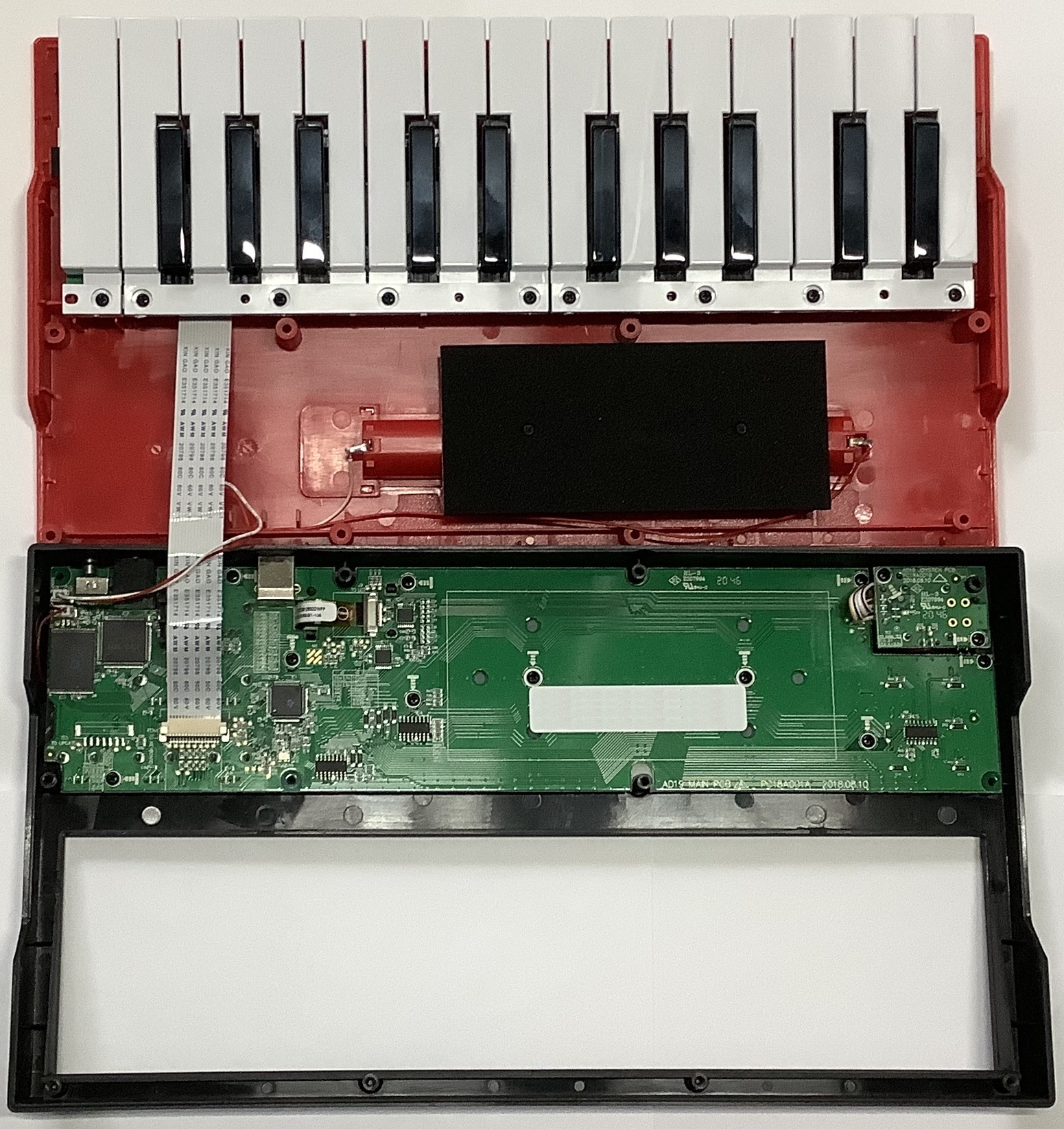
As you can see in the picture, the keybed is mounted on the bottom tray. The battery compartment is molded into the bottom. A ribbon cable connects the keybed switch matrix (rows and columns) to the main PCB. In the future, I’d like to personalize my Mini Play by replacing the standard black on white keybed with a white on black keybed — Vox Continental envy. 🙂
The main PCB has left, middle and right parts. The middle looks empty, but the rhythm pads are on the other side in this region. The rubbery black pad in the case bottom provides mechanical support to the PCB beneath the rhythm pads.
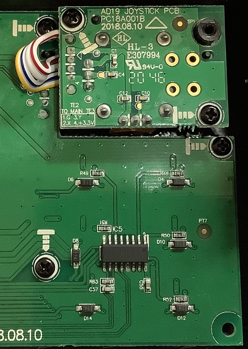
The right part of the main PCB has the arpeggiator switches and joystick subassembly. The legend on the integrated circuit (IC) is super faint and is barely readable with a strong light and magnifying glass. IC5 appears to be a CMOS 595D 8-bit serial-in, serial- or parallel-out shift register. Signals from the right part of the PCB travel over a gazillion traces to the left part.
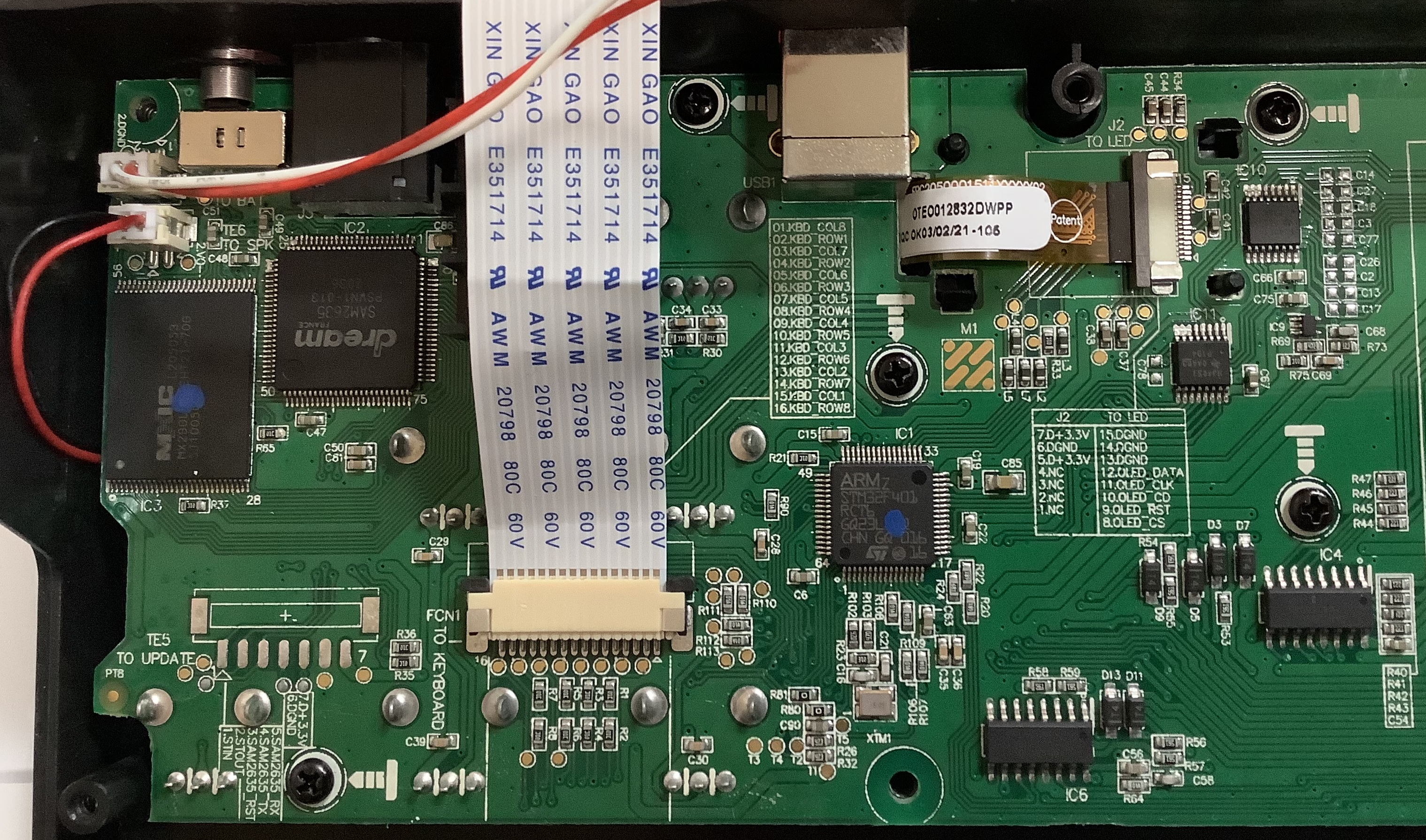
All the really fun stuff is on the left part of the main PCB. Here you will find the back panel components: battery/USB power switch, 3.5mm headphone jack, sustain pedal jack, and USB-B port. The sustain pedal jack is hidden beneath the ribbon cable in the picture. [You’re not really missing anything.]
The ribbon cable near the USB-B connector connects the OLED display to the main PCB. IC10 and IC11 are TI HJ4051 8:1 multiplexer/demultiplexers. Akai conveniently printed cable signal tables on the PCB. Signals for the OLED display (J2) are:
     Pin Signal       Pin Signal
     --- ---------    --- ---------
      1  NC             8 OLED_CS
      2  NC             9 OLED_RST
      3  NC            10 OLED_CD
      4  NC            11 OLED_CLK
      5  D +3.3V       12 OLED_DATA
      6  D GND         13 D GND
      7  D +3.3V       14 D GND
                       15 D GND
The legends on IC4 and IC5 are quite faint. They are either 74HC595D or 74HC395D. My eyes are old and sore. 🙂 This logic is probably related to the rhythm pads and signals from the right side of the main PCB.
Signal assignments are given for the keybed ribbon cable (FCN1):
     Pin Signal       Pin Signal
     --- ---------    --- ---------
      1  KBD_COL8       9 KBD_COL4
      2  KBD_ROW1      10 KBD_ROW5
      3  KBD_COL7      11 KBD_COL3
      4  KBD_ROW2      12 KBD_ROW6
      5  KBD_COL6      13 KBD_COL2
      6  KBD_ROW3      14 KBD_ROW7
      7  KBD_COL5      15 KBD_COL1
      8  KBD_ROW4      16 KBD_ROW8
Typical key scanning drives a row (or column) signal and reads back a column (or row) group. Holy smokes! The Mini Play PCB may support eight groups of eight keys. If the proper software support is implemented, one might be able to attach a 61-key keybed to the main PCB! (A big “IF”.)
The 64 pin surface mount (SMT) device near the two printed tables is the main CPU: an ST Microelectronics STM32F401RCT6 Arm Cortex-M4 microcontroller. This device has a single core, 64KB RAM and 256KB flash memory. The blue dot may indicate that the device was programmed before installation. (Dunno.) I can’t read the top of the crystal XTIM1, so I don’t know the clock speed.
Finally, we get to the synthesizer (IC2): a Dream S.A.S. SAM2635. The Macronix IC (IC3) at the left edge of the PCB is NOR flash containing the Dream waveforms. Again, the blue dot may signify preload status. Near the SAM2635, we find JST connectors for the battery and the speaker.
In my view, the most exciting and interesting part of the main board are the test points in the lower left corner. The signals are:
    Pad Signal        Dream function
    --- -----------   ---------------------------
     1  STIN          Serial test input
     2  STOUT         Serial test output
     3  SAM2635_RST   Master reset and power down
     4  SAM2635_TX    MIDI OUT
     5  SAM2635_RX    MIDI IN
     6  D GND         Digital ground
     7  D +3.3V       Digital +3.3V
I verified these connections using a continuity tester. The SAM2635_RX and SAM2635_TX pads are connected to the Arm microcontroller:
    Pin  Function       Test POINT  Pad
    ---  ------------   ----------  ---
     42  USART1_TX      SAM2635_RX   5  I/O 5V tolerant
     43  USART1_RX      SAM2635_TX   4  I/O 5V tolerant
So, boys and girls, we may be in business!
In my opinion, Akai botched the MPK Mini Play by hiding the Dream synthesizer behind software on the Arm. The Arm makes the Mini Play look like a semi-crazed synth of its own, not the SAM2635. The test points may — may — provide a way to get at the Dream synthesizer directly. The INTERNAL SOUNDS button acts like a MIDI LOCAL CONTROL button. So, I’m hoping to disable internal sounds and hijack the MIDI IN and OUT test pads (signals) to the SAM2635.
Come for the teardown; Stay for the mods:
- Bring out the MPK Mini Play MIDI signals
- Monitor internal MPK Mini Play MIDI messages
- Jam with Akai MPK Mini Play 5-pin MIDI IN and MIDI OUT
- Communicate with Akai MPK Mini Play MIDI over USB
Copyright © 2022 Paul J. Drongowski