About pj

Now (mostly) retired, I'm pursing electronics and computing just for the fun of it! I'm a computer scientist and engineer who has worked for AMD, Hewlett Packard and Siemens. I also taught hardware and software development at Case Western Reserve University, Tufts University and Princeton. Hopefully, you will find the information on this site to be helpful. Educators and students are particularly welcome!

ARM Cortex-A72 execution and load/store

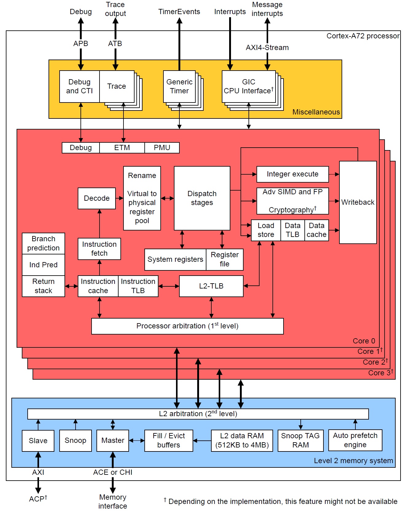
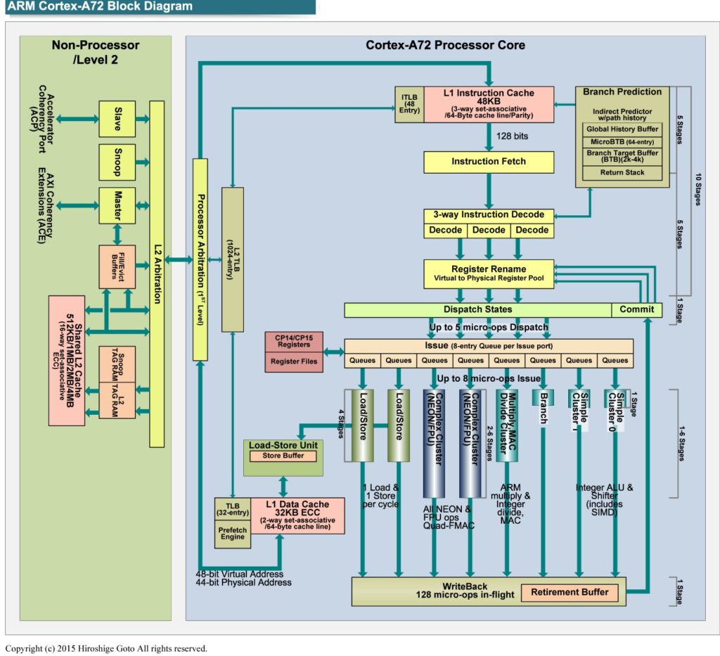
I hope you had an opportunity to read about ARM Cortex-A72 fetch and processing. ARM Cortex-A72 is the high performance application core in the Broadcom BCM2711, also known as the Raspberry Pi 4. In this post, I’m going to continue my exploration of the A72 micro-architecture, concentrating on the execution units and load/store operation.

Execution pipelines

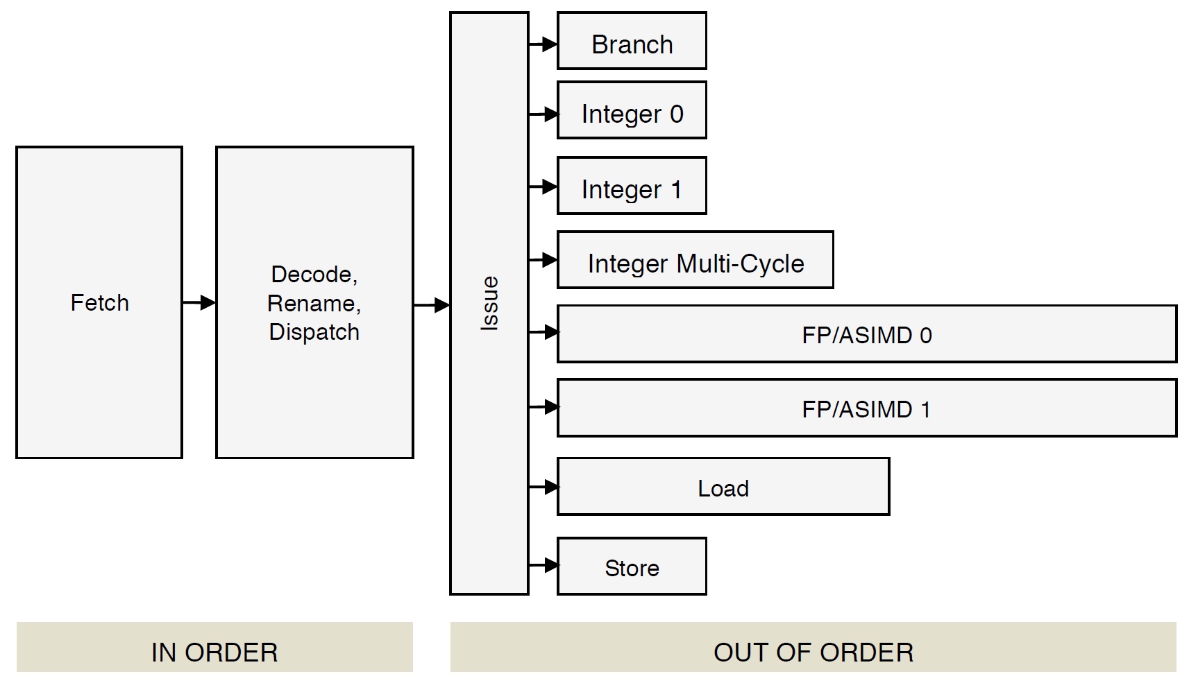
Cortex-A72 has eight independent execution units (pipelines):

  • Branch: Branch micro-ops
  • Integer 0: Integer ALU micro-ops
  • Integer 1: Integer ALU micro-ops
  • Integer Multi-Cycle: Integer shift-ALU, multiply, divide, CRC and sum-of-absolute differences micro-ops
  • FP/ASIMD 0: ASIMD ALU, ASIMD misc, ASIMD integer multiply, FP convert, FP misc, FP add, FP multiply, FP divide and crypto micro-ops
  • FP/ASIMD 1: ASIMD ALU, ASIMD misc, FP misc, FP add, FP multiply, FP square root and ASIMD shift micro-ops
  • Load: Load and register transfer micro-ops
  • Store: Store and special memory micro-ops

The Cortex-A72 front-end puts micro-ops into per-pipe issue queues which, in turn, feed the execution units. There are eight issue queues. The queues have eight entries each except the branch queue, which has ten entries (66 queue entries total like the old Cortex-A57). The queues provide rate-balancing between the core front-end (i.e., the instruction/micro-op stream) and the execution units. The queues allow greater parallelism between units, too, letting each pipeline run at its own independent single- or multi-cycle speed.

ARM Cortex-A72 micro-architecture (Source: Hiroshige Goto)

The branch and integer pipes are very fast, each pipe executing a micro-op in a single processor cycle. The integer pipelines have multiple, zero-cycle forwarding datapaths. These paths, sometimes called “by-passes,” send intermediate results directly to stages (computations) needing the result right darned now without writing the result into the rename register file first.

The integer multi-cycle pipe handles integer micro-ops which require 2 or more processor cycles for execution. Shift operations are relatively fast: 2+ cycles. Integer multiplication has a 3 to 5 cycle latency. Integer divide is relatively slow taking anywhere from 4 to 20 cycles. Multiplication can be accelerated through dedicated combinational logic; division is sequential by nature and requires many steps.

The FP (floating point) and ASIMD (Advanced Single Instruction Multiple Data) units perform floating point and SIMD computations. Both units are generalist and perform commonly occurring FP operations: FP ADD, SUB, MUL, NEG, ABS, MAX, MIN, etc. Execution latency varies from 3 to 4 cycles for these basic operations. The FP pipes support late forwarding of FP MUL products to FP multiply-accumulate micro-ops, letting FP multiply-accumulate complete in 6 cycles.

Each FP unit is a specialist, too:

  • FP/ASIMD 0: FP CONVERT, ROUND, DIV, CRYPTO
  • FP/ASIMD 1: FP COMPARE, SQRT

FP divide and square root operations are performed using iterative algorithms. Only one FP DIV or SQRT operation at a time may execute in a pipe. Latencies are long: 6 to 18 cycles for DIV and 6 to 32 cycles for SQRT, depending upon FP datatype.

Please see the ARM Cortex-A72 Software Optimization Guide for detailed instruction timing, pipe assignment and ASIMD operation.

Load and store micro-ops are executed by the load and store units. The load and store units are mutually independent. One load and one store micro-op can execute each processor cycle. (Load and store are discussed below.) Load and store micro-ops issue speculatively. Under speculative execution, a load or store may reside on a correctly predicted branch path (the correct path) or an incorrectly predicted branch path (the wrong path). Loads, stores and associated data on a wrong path must be discarded. Store operations are buffered (wait) until they are determined to be on the correct path and are committed architecturally to primary memory.

Memory hierarchy

As I mentioned in my Cortex-A72 overview, the Raspberry Pi 4 (Broadcom BCM2711) has a four level memory hierarchy:

          Register          Fast, but small 
|
Level 1 caches
|
Level 2 cache
|
RAM Big, but slow

The RPi4 has four A72 cores. Each core has a register file and level 1 instruction and data caches. The four cores share a single unified level 2 cache and primary memory (RAM).

The register file is the fastest, but has the smallest capacity. Registers are read or written in a single processor cycle. RAM has the most capacity, but is relatively slow. RPi4 primary memory is LPDDR4-3200 SDRAM:

Memory array clock200 MHz
Prefetch size16n
I/O bus clock frequency1600 MHz
Data transfer rate (DDR)3200 Mb/s
Memory accesss bandwidth (MABW)12.8 GB/s

MABW above is peak. Memory bandwidth measurements using RAMspeed/SMP indicate actual RPi4 model B bandwidth is approximately 4.4 GB/s. (RAMspeed/SMP reads/writes memory in 1MB blocks.)

The following table summarizes Cortex-A72 cache characteristics:

L1I cache capacity48KB
L1I cache organizationPer-core, 3-way set associative, 64B line
L1D cache capacity32KB
L1D cache organizationPer-core, 2-way set associative, 64B line
L2 cache capacity1MB
L2 cache organizationShared, 16-way set associative, 64B line

Data accesses are handled by the Level 1 Data (L1D) cache. Instruction fetches are handled by the Level 1 Instruction (L1I) cache. The Level 2 (L2) cache is unified, handling both data and instructions. The Raspberry Pi BCM2711 ARM Peripherals manual states the following caveat with respect to the L2 cache:

BCM2711 provides a 1MB system L2 cache, which is used primarily by the GPU. Accesses to memory are routed either via or around the L2 cache depending on the address range being used.

Thus, application programs should not expect to receive a performance assist from the L2 cache! The VideoCode GPU accesses L2 cache through the Cortex-A72 ACP/AXI interface.

The L1D cache load-to-use latency is 4 cycles when the load hits in the L1D cache. The Level 2 (L2) cache load-to-use latency is 9 cycles when the load hits in the L2 cache.

A read access (e.g., a data load or instruction fetch) first tries the appropriate level 1 cache (Load: L1D cache, Fetch: L1I cache). If it finds the requested item in the level 1 cache — a hit — the item is sent to either the rename registers (for loads) or the instruction decoder (for fetches). Load data may also be sent through a bypass to an execution stage (micro-op) awaiting the incoming data.

If the read access misses the level 1 cache, the request is sent (optionally) to the unified L2 cache. If the requested item is found in L2 cache, the cache line containing the item is written into the level 1 cache, thereby replacing one of the existing lines. This operation is called a “refill.” If the line to be replaced is dirty (modified), then the old value is evicted and is written to primary memory. The requested item is selected from the incoming cache line and is routed to the appropriate destination (i.e., functional unit or instruction decoder).

If the read access misses (or optionally, bypasses) the L2 cache, the 64 byte line containing the item is read from primary memory. The incoming line is written to the level 1 cache (a refill) and (optionally) the L2 cache. Again, dirty lines are evicted.

Instruction and data bytes are read, written and transferred in 64-byte chunks (lines). This is true even if a load instruction requests a single byte from memory. Application programs should strive to use each entire cache line completely before moving on to the next line. Programs that exploit spatial and temporal locality perform better. Programmers need to pay careful attention to algorithm selection, data structure/layout and memory access patterns in order to make good, efficient use of data caching.

The description of Cortex-A72 cache operation above is simplified. Consider, for example, memory transaction types. Memory attributes within the Memory Management Unit (MMU) and page tables determine memory transaction types for each memory region:

  • Write-Back Read-Write-Allocate
  • Write-Back No-Allocate
  • Write-Through
  • Non-cacheable
  • Device

Memory transaction type affects cache behavior.

Write-Back Read-Write-Allocate is the most common and highest performing memory type. Incoming lines are written to the L1D cache and the read (or write) completes from the L1D cache. A store that hits a Write-Back cache line does not update main memory.

Write-Back No-Allocate does not write an incoming line to L1D cache. This prevents cache pollution when accessing large, one-time use data structures.

Non-cacheable memory bypasses both the level 1 caches and L2 cache. Requests go directly to primary memory. The Cortex-A72 treats Write-Through memory as Non-cacheable.

Instruction fetch (more details)

Instruction fetches are speculative and there is no guarantee that fetched instructions are executed. Instructions are aggressively prefetched pursuing either sequential execution flow or branch targets based on path prediction.

The L1I cache is fed by three fill buffers that hold instructions from either the unified L2 cache or primary memory. The fill buffers are non-blocking. A line may remain in a fill buffer until it is transferred to the L1I cache or discarded. Primary memory regions may be marked as non-cacheable regions or the L1I cache may be disabled, and incoming lines are not written to the L1I cache. A line is not committed to the L1I cache unless it is demanded by a fetch. The hardware also has an L2 instruction prefetcher.

Cortex-A72 treats the preload instruction cache instruction (PLDI) as a NOP.

Memory Management Unit

The Memory Management Unit (MMU) performs virtual to physical address translation and enforces secure, restricted access to memory regions. As to security, suffice it to say that the MMU restricts access by Address Space Identifier (ASID) and Virtual Machine Identifier (VMID). These concerns are addressed by the operating system and are generally transparent to application programmers. [And I won’t be dealing with access control here.]

Address type AArch64 AArch32
Virtual address (VA)48 bits 32 bits
Physical address (PA)44 bits 40 bits

The Cortex-A72 hardware supports 4KB, 64KB and 1MB page sizes. The Raspberry Pi Operating System (formerly known as “Raspbian”) organizes primary memory into 4KByte pages. [Huge pages must be enabled in the kernel and I will assume that it’s 4KB all the way on RPi4.] The operating system maintains page tables that specify the physical location of application program pages (both instructions and data).

Application programs use virtual addresses to identify instructions and data items. Conceivably, hardware could use memory-resident page tables to map a virtual address to its corresponding physical address. This approach is way too slow to be practical. Better, the Cortex-A72 maintains page (address) mapping information in a multi-level, hierarchical memory system:

       Level 1 TLB          Fast, but small 
|
Level 2 TLB
|
RAM Big page tables, but slow

The TLB structure is separate from the register/cache/memory hierarchy and it operates independently. The organizing principle is the same — most recent and frequently used mappings reside in fast memory and big page tables reside in slow primary memory.

“TLB” is the acronym for “translation lookaside buffer.” A TLB is an array where each entry describes the mapping from a virtual page to a physical page. Internal operation of a TLB is similar to a data cache. The following table summarizes Cortex-A72 TLB characteristics:

L1I TLB capacity48 entries
L1I TLB organizationFully associative
L1D TLB capacity32 entries
L1D TLB organizationFully associative
L2 TLB capacity1024 entries
L2 TLB organization4-way set associative

The L1I and L2D TLBs support 4KB, 64KB, and 1MB page sizes. The L2 TLB supports 4KB, 64KB, 1MB and 16MB page sizes. (Also, 2MB and 1GB using AArch32 long descriptor format translation.) Alas, Raspberry Pi OS uses 4KB pages.

TLB operation is similar to caching. Address translation is first tried in the L1I TLB (fetches) or L1D TLB (loads and stores). If the translation information is found (a hit), the physical address is returned in one cycle. Access permission is checked at the same time.

If translation misses in a level 1 TLB, address translation is attempted in the main L2 TLB. If the translation information is found, the physical address is returned (after one or more cycles).

If translation misses in the L2 TLB, the MMU performs a hardware translation table walk. (Page tables have a fairly complicated structure which is beyond the scope of this discussion.) Because page tables reside in slow primary memory, a hardware translation table walk takes a relatively long time to complete with respect to an L2 TLB look-up.

If the required page is not in memory and is on the RPi OS swap device, the operating system reads the page into primary memory before attempting re-translation. These exceptions, page faults, are the slowest of all and they should be avoided like the plague.

Once again, program performance depends up good temporal and spatial locality, albeit locality at the page level. An application program can touch as many as 32 different data pages without triggering an L1D TLB refill:

    32 L1D TLB entries * 4 KBytes/page = 128 KByte data working set

This is a modest-sized working set of pages, and like cache line strategy, a program should make maximal, efficient use of a page working set before demanding new page translation information from the L2 TLB. The L2 TLB supports a larger combined data/instruction working set:

   1024 L2 TLB entries * 4 KBytes/page = 4 MByte total working set 

The L2 TLB footprint (working set size) is larger. However, the L1D TLB and the L1I TLB compete for page translation entries in the unified L2 TLB.

As to data-page utilization, data structure layout and access pattern come into play once again. A program should work as much as possible within the current working set before moving to pages outside the current set. Random access within a big heap pays a penalty when heap items are distributed across many pages (i.e., when the working set exceeds 32 pages).

With respect to L1I TLB utilization strategy, frequently executed, related code should reside within the same page or just a few pages. Related code which is spread across many pages (i.e., a large instruction working set) will jump between pages and possibly cause L1I TLB or L2 TLB refills.

The above description of the translation process is simplified. For example, access is checked against page permissions, etc. and violations are reported after aborting offending translation and instruction. I tried to focus mainly on performance-related concerns of interest to application programmers.

Load and store operations

After absorbing all of that, let’s pick up a few additional odds and ends about load and store operations.

Cortex-A72 memory operations are weakly ordered. They may be performed out-of-order as long as data dependencies are honored. Due to the weak ordering, explicit synchronization barriers are needed in circumstance where strong ordering is required. There are four kinds of barriers:

  • Instruction Synchronization Barrier (ISB)
  • Data Synchronization Barrier (DSB)
  • Data Memory Barrier (DMB)
  • Load-Acquire (LDAR) and Store-Release (STLR)

Please see the Programmer’s Guide for ARMv8-A for further details.

More generally important to application programmers is data alignment. Naturally aligned data is accessed faster than unaligned data, especially unaligned data items that cross cache line boundaries. The following table summarizes alignment requirements:

Source: Programmer’s Guide for ARMv8-A

Load operations should not cross 64-byte, cache line boundaries. Store operations should not cross 16-byte boundaries.

As a general program design principle, computations proceed as fast as data items can stream from primary memory, and secondarily, as fast as results can stream back to primary memory. Data prefetching increases the speed of incoming data stream(s). The programmer or compiler should schedule load operations further ahead of instructions which consume the incoming data item. Ideally, other independent instructions are scheduled and executed ahead of the consuming load thereby overlapping useful computation with load latency (4 cycles from the L1D cache at a minimum).

A program may signal the need for a data item through an explicit prefetch instruction. The A72 supports three instruction prefetch hint instructions: PLD, PLDW, and PRFM. These are only hints and may be ignored. The PLD and PLDW instructions allocate a line in the Level 1 Data cache. Prefetch from Memory (PRFM) hints that data from a specific address will soon be needed. If accepted, these hints can bring in a data item (cache line) before it is required.

Programmers may further manage data cache contents via non-temporal load and store instructions (LDNP and STNP). These instructions hint that caching is not useful for data at an address, thereby preventing unnecessary cache pollution. Non-temporal load and store instructions may require explicit load barriers. (See the Programmer’s Guide for ARMv8-A for more details.)

The Cortex-A72 hardware has a load-side prefetcher which dynamically analyzes memory access patterns. Based on its analysis, the load-side prefetcher brings data into either the L1D cache, the L2 cache, or both. The hardware also has a store-side prefetcher which brings data into the L2 cache.

Outgoing data streams benefit from write combining which merges data from multiple store operations into a single memory write access.

Outstanding read and write requests (i.e., pending requests to primary memory) wait in the Fill/Eviction Queue (FEQ). The Cortex-A72 has a configurable FEQ: 20, 24, or 28 entries. The A72 write issuing capability is 16, that is, up to 16 writes may be outstanding at any time. The read issuing capability is 19, 23, or 27 depending upon FEQ configuration (capacity). L2 prefetch is throttled based on the FEQ occupancy count. [Extra credit: What is the specific Raspberry Pi 4 FEQ configuration and occupancy threshold?]

One important simplification in the cache discussion is cache coherency. Most application programmers needn’t worry about cache coherency. However, if you are writing a program with multiple, co-operating threads that actively share memory locations or regions, you should MOESI over to the ARM Cortex-A72 Technical Reference Manual (TRM) and read up on the details. The A72 Snoop Control Unit (SCU) uses a hybrid protocol (MESI+MOESI) to maintain coherency between the per-core L1 data caches (MESI) and the common L2 cache (MOESI). “MESI” and “MOESI” refer to the coherency status of each cache line:

  • Modified (M)
  • Owned (O)
  • Exclusive (E)
  • Shared (S)
  • Invalid (I)

The BCM2711 employs an Advanced Microcontroller Bus Architecture (AMBA) Advanced xExtensible Interface (AXI) bus interface. Broadcom does not specify if either AXI Coherency Extensions (ACE) or the Coherency Hub Interface (CHI) are supported. (Man, these acronyms stack up!) Since ACE and CHI are intended for SMP processor clusters (e.g., big.LITTLE) these features may have been left out or disabled.

If you do care about cache coherency, please be aware that load data may be sourced from a remote L1D cache as well as the shared L2 cache or primary memory.

Sources

Before closing, I want to offer a few words about my sources. My primary resources are:

  • ARM Cortex-A72 Technical Reference Manual (TRM)
  • ARM Cortex-A72 Software Optimization Guide
  • ARM Programmer’s Guide for ARMv8-A
  • BCM2711 ARM Peripherals

These resources are authoritative. I also relied upon ARM’s own briefings and presentations about Cortex-A72 as found on the Web. I tried to verify Web sources and briefings against the written TRM and programmer guides.

In closing

Hopefully, my write-ups will help developers tune their programs for ARM Cortex-A72. If you’re just getting started with performance tuning, I would first concentrate on cache- and page-friendly algorithms, data structures and access patterns. Fill buffers, FEQ, memory ordering, and memory transaction types are esoteric subjects for most application programmers.

Want to learn more about Raspberry Pi 4 (Cortex-A72 / Broadcom BCM2711) performance tuning? Please read:

If you’re interested in early model Raspberry Pi, I wrote several posts about micro-architecture, performance measurement and performance events:

There you will find general principles and techniques that apply to Raspberry Pi 4 although some details (e.g., cache and TLB capacity) differ.

Copyright © 2021 Paul J. Drongowski

ARM Cortex-A72 fetch and branch processing

Let’s take a closer look at instruction fetch, decode and dispatch in the Cortex-A72 micro-architecture. These are the “front-end” stages of the core pipeline. The “back-end” of the pipeline consists of the register file(s), execution units and retirement (reorder) buffer. Branch prediction is frequently associated with the front-end since it directly affects instruction fetch.

[Update: This post is part 1 of a two part series. Part 2 discusses ARM Cortex-A72 execution and load/store operations.]

The front-end has one major job: Fetch ARMv8 instructions and keep the back-end execution units as busy as possible.

This page is required reading for Raspberry Pi 4 (BCM2711, ARM Cortex-A72) programmers who want to tune their programs for the ARM Cortex-A72. It is also necessary background information for programmers doing performance measurement with PERF (Performance Events for Linux) on Raspberry Pi 4.

Fetch, decode and dispatch

The Cortex-A72 pipeline has 15 stages. [On-line sources disagree on the length; some sources claim 14 stages.] The front-end stages are:

  • Fetch (5 stages)
  • Decode (3 stages)
  • Rename (1 stage)
  • Dispatch (2 stages)

The back-end pipeline stages are:

  • Execute (1 to 6 stages depending upon unit)
  • Write-back/retirement (2 stages)

Each execution unit has its own pipe:

  • Integer 0 (1 stage/cycle)
  • Integer 1 (1 stage/cycle)
  • Integer multi-cycle (4 to 12 cycles)
  • FP/ASIMD 0 (6 to 18 cycles)
  • FP/ASIMD 1 (6 to 32 cycles)
  • Load L1D cache hit: 4 cycles)
  • Store (1 cycle)
  • Branch (1 cycle)

See the ARM Cortex-A72 software optimization guide for exact instruction execution latencies.

ARM Cortex-A72 pipeline (Cortex-A72 Software Optimization Guide)

70 plus years after von Neumann, we still adhere to a linear, sequential program model. In the programmer’s view, there is a program counter (PC) which steps through instructions sequentially, even if some of the intended high-level computations could be performed in parallel by the execution units. Further, we force compilers to lay down instructions in the same linear, sequential fashion.

The front-end’s job is to find instruction-level parallelism (ILP) within the incoming instruction stream. The Cortex-A72 front-end translates ARMv8 instructions into micro-ops. It sends the micro-ops to the back-end functional units for execution and architecture-level retirement.

This all may seem inefficient and crazy and it is. Program representation and execution need a major re-think along the lines of the once-investigated dataflow architecture. Why do and then un-do?

Front-end translation is really two steps: translating ARMv8 instruction into macro-ops and then translating macro-ops into micro-ops. Let’s examine the details.

First, fetch acquires a 16-byte (128 bit quadword) fetch window and it recognizes ARMv8 instructions within the window (and across windows). Then, the decode stages turn the ARMv8 instructions into one or more macro-ops. The decoder will fuse multiple ARMv8 instructions into a single macro-op if such an optimization is possible. Architectural registers are renamed to an internal register file which temporarily holds intermediate results. Next, the macro-ops are translated into micro-ops and the micro-ops are dispatched to the issue queue belonging to the appropriate functional unit. Micro-ops are dispatched into 8 independent issue queues (one queue per execution pipeline). When an instruction successfully completes, it is retired and its result is committed to the architectural machine state. [I will discuss the meaning of “successfully completes” in a minute.]

There are limits on the number of ARMv8 instructions, macro-ops and micro-ops which are processed during a machine cycle:

    3 ARMv8 instructions --> 3 macro-ops --> 5 micro-ops 
Decode Rename Dispatch

During each cycle, the Cortex-A72 can decode 3 ARMv8 instructions, produce up to 3 macro-ops and dispatch up to 5 micro-ops. There are additional limitations on the number of micro-ops of each type that can be simultaneously dispatched (quoting the Cortex-A72 software optimization guide):

  • One micro-op using the Branch pipeline
  • Up to two micro-ops using the Integer pipelines
  • Up to two micro-ops using the Multi-cycle pipeline
  • One micro-op using the F0 pipeline
  • One micro-op using the F1 pipeline
  • Up to two micro-ops using the Load or Store pipeline

If there are more micro-ops to be dispatched above these limitations, they are dispatched in oldest-to-youngest age order.

According to ARM, most ARMv8 instructions are converted to a single micro-op (average: 1.08 micro-ops per instruction).

Register renaming allows micro-ops to execute out-of-order. Remember, we forced the compiler to lay down ARMv8 instructions in-order. Register renaming allows the micro-ops to execute out-of-order without violating data dependencies between architectural registers. There are 128 physical rename registers.

Speculative execution

Now the really tricky stuff — speculative execution. A basic block is a sequence of “straight-line” code with a single branch instruction at the end of the block. Program control flows into a basic block and is redirected at the end to either the same basic block or perhaps a different basic block.

Generally, basic blocks are about 9 instructions long. The branch at the end may be a conditional branch. The combination of short block length and conditional branching limits the number of ARMv8 instructions which can be aggressively fetched, decoded and dispatched within a single basic block. Without speculative execution, the processor must wait every time a conditional branch needs to be decided.

Enter branch prediction. When Cortex-A72 hits a conditional branch, it predicts the direction: taken or not taken. [More about branch prediction in a minute.] The front-end continues to fetch, decode and dispatch along the predicted control flow path. If the prediction is correct, hurray! The predictor has guessed correctly and the execution units have already been computing useful results. As each ARMv8 instruction completes along a known-to-be correct path, the instructions along the path retire in architectural order. This is the meaning of “successfully completes” above.

If a conditional branch is not predicted correctly (a “mispredict”), the intermediate results along the wrong path are discarded and the fetch stage is told to start fetching from the correct target address. This is called a “re-steer” as in the phrase “re-steering the front-end.” Recovery from a branch mispredict requires a pipeline flush and, yes, it’s expensive — at least 15 cycles.

The Write-back/retirement stage keeps track of the “retire pointer,” that is, the architectural program counter. The retirement stage is some of the most difficult hardware logic to design and it must be correct. The retirement stage maintains a reorder buffer which keeps the books on instruction and micro-op status. The reorder buffer has 128 entries, allowing up to 128 ARMv8 instructions to be simultaneously in flight.

Branch prediction

High performance rides on branch prediction accuracy. If the predictor guesses correctly most of the time, then speculative execution is a win. If the predictor guesses incorrectly, the core must throw away useless results and the execution pipeline stalls.

A deep dive into branch prediction is beyond the scope of this note. So, here’s a sketch. The predictor maintains a Pattern History Table (PHT) which retains the taken or not-taken status of (recent) branches encountered by the core. The predictor also maintains a Branch Target Buffer (BTB) containing the target addresses of these branches. The predictor uses the pattern history to predict the direction of a branch when it encounters the branch again. The BTB supplies the associated target address.

Cortex-A72 allows split BTB entries, accomodating both near branches (small target address) and far branches (large target addresses). That’s why you will see the BTB capacity quoted as 2K to 4K entries. The A72 BTB can hold as a many as 2K large target address (far) and 4K small target addresses (near). The A72 also has a micro-BTB which acts as a cache memory for the main BTB. The micro-BTB has 64 entries.

The branch prediction window is 16 bytes, which has implications for basic block layout. According to the Cortex-A72 software optimization guide, branch targets should be quadword aligned (i.e., 16 byte boundaries) and not more than two taken branches should be included with the same quadword-aligned quadword of instruction memory.

The compiler should really take care of quadword alignment and packing for you. As a higher-level language programmer, you can improve branch prediction by biasing flow conditions toward a true program path or the respective false program path. If a given path (true if-clause or false if-clause) is more frequently executed, the branch predictor should do a better job predicting the underlying conditional branch generated by the compiler.

Cortex-A72 has predictors for subroutine return and indirect branch. The predictor maintains an 8 [?] entry Call/Return Stack which remembers the most recent return addresses. Measurement shows that 8 entries (or so) are enough for most high-level language workloads, covering the most recently called functions.

Bi-mode prediction

There are three sources of interference in a Pattern History Table (PHT):
* Cold miss (compulsory alias)
* PHT capacity miss (capacity alias)
* Conflict miss (conflict alias)
Conflict misses can be reduced by partitioning the PHT or using a different
indexing scheme.

The ARM Cortex-A15 Bi-Mode predictor uses two pattern history tables and a choice predictor to reduce negative interference of branches in different
program modes. Instead of one big PHT, the pattern history is partitioned
into two halves, i.e., two smaller PHTs. A choice predictor table selects
one of the two PHTs. The chosen side delivers the final prediction.

Cortex-A72 does not employ a bi-mode predictor. In case you’re wondering, Cortex-A72 does not have a micro-op loop buffer either.

Want to learn more about Raspberry Pi 4 (Cortex-A72 / Broadcom BCM2711) performance tuning? Please read:

If you have an early model Raspberry Pi, read about the ARM11 micro-architecture here. Please don’t forget my PERF (Performance Events for Linux) tutorial.

Copyright © 2020 Paul J. Drongowski

A short trip through ARM cores

Digging around in the kernel and PERF source code, I got lost in the labyrinth of ARM products. So, I took a little time to learn about ARM’s naming conventions.

ARM have always been good at separating architecture and implementation (code technology). Architecture is what the programmer sees, rather, the behavioral standard which includes the “instruction set architecture” or “ISA.” Architecture goes beyond instruction sets and includes operating system concerns such as virtual memory, interrupts, etc.

Core technology implements architectural features. Core technology is the underlying machine organization AKA the “micro-architecture.” Depending upon the actual design, Implementation touches on pipeline length and stages, caches, translation look-aside buffers (TLB), branch predictors and all of the other circuit stuff needed for efficient, performant execution.

ARM architecture names have the form “ARMvX”, where X is the version number. The original Raspberry Pi (Broadcom2835 with ARM1176JZF-S processor) implemented the ARMv6 architecture. The current Raspberry Pi 4 (Broadcom BCM2711 with quad Cortex-A72 cores) implements the ARMv8-A architecture. ARMv8 is a multi-faceted beast and a short summary is wholly inadequate to convey its full scope. I suggest reading through the ARMv8 architectural profile on the ARM Web site. Suffice it to say here, ARMv8.2 is the latest.

ARMv8 was and is a big deal. ARMv7 was 32-bit only. ARMv8 took the architecture into 64-bit operation while retaining ARMv7 32-bit functionality. ARMv8 added a 64-bit ISA and operating system features, separating operation into the AArch32 execution state and the (then) new AArch64 execution state. It preserves backward compatibility with ARMv7.

You probably noticed that the core name “ARM1176JZF-S” (above) is neither the most informative nor does it suggests this core’s place in the constellation of ARM products. In 2005, ARM introduced a new core technology naming scheme. The naming scheme categorizes cores by series:

  • Cortex-A: Application
  • Cortex-R: Realtime
  • Cortex-M: Embedded

The series letters spell out “ARM” — clever. Cores within a series are tailored for their intended deployment environment having the appropriate mix of performance (speed), real estate (space) and power envelope.

The following table is a partial, historical roadmap of recent ARM cores:

    32-bit cores       64-bit cores (ARMx8) 
------------ ----------------------------------
Cortex-A5 Cortex-A53 2012 In-order LITTLE
Cortex-A7 Cortex-A57 2012 Out-of-order big
Cortex-A8 Cortex-A72 2015 Out-of-order big
Cortex-A9 Cortex-A73 2016 Out-of-order big
Cortex-A12 Cortex-A55 2017 In-order LITTLE
Cortex-A15 Cortex-A76 2018 Out-of-order big
Cortex-A17 Cortex-A77 2019 Out-of-order big

The 64-bit cores in the second column are a significant architectural break from the 32-bit cores in the first column. I will focus on the ARMv8 (64-bit) cores.

ARM rolled out big.LITTLE multiprocessor configuration at roughly the same time as ARMv8. With big.LITTLE, ARM vendors can design multiprocessors that are a mixture of big cores and LITTLE cores. LITTLE cores are power-efficient implementations much like ARM’s previous core designs for embedded and mobile systems — systems which consume and dissipate as little power as possible. Big cores trade higher power for higher performance. [If you really want to make digital electronics go fast, you must expend energy.] The big.LITTLE approach allows a mix of power-efficient cores and high-performing cores in a multicore system. Thus, a cell phone can spend most of its time in low power cores saving battery while hitting the high power cores when compute performance is required by the user.

The big.LITTLE approach is enabled by common cache and coherent communication bus design. The little guys and the big guys communicate through a common infrastructure. Nice.

ARMv8 LITTLE cores are in-order superscalar designs. In-order designs are simpler than out-of-order superscalar. In-order cores usually have a shorter pipeline, have fewer execution units, and do not require a big register file for renaming and delayed retirement. Out-of-order superscalar designs pull out all of the stops for performance and exploit as much instruction level parallelism (ILP) as they can discover.

The Cortex-A53 was the first ARMv8 in-order LITTLE core. ARM introduced its successor, Cortex-A55, in 2017.

The big core era began with Cortex-A57. This was ARM’s first design that rivaled Intel and AMD out-of-order x86 cores. The Cortex-A72 replaced the A57. Thus, the Raspberry Pi 4 (BCM2711) uses an older ARM big core, the Cortex-A72. [Explains my enthusiasm for a $70 o-o-o superscalar.] ARM have churned out new big cores on an annual basis ever since from its Austin and Sophia design centers.

Before pushing ahead, it’s worth mentioning that the Yamaha Montage synthesizer has an 800MHz Texas Instruments Sitara ARM Cortex-A8 single core processor and a 40MHz Fujitsu MB9AF141NA with an ARM Cortex-M3 core. The four 64-bit A72 cores in the Raspberry Pi 4 have much more compute throughput than the single 32-bit A8 core in the Yamaha Montage. The Montage (MODX) processor provides user interface and control and is not really a compute engine. The SWP70 silicon is the tone generator.

In practice

I began this dive into naming and ARM cores when I needed to determine the actual ARM core support installed with Performance Events for Linux (PERF) and the underlying kernel.

The kernel creates system files which let a program query the characteristics of the hardware platform. You might be familiar with the /proc directory, for example. There are a few such directories associated with the kernel’s performance counter interface. (See the man page for perf_event_open().) The directory:

    /sys/bus/event_source/devices/XXX/events

lists the performance events supported by the processor, XXX. In the case of the Raspberry Pi 4, XXX is “armv7_cortex_a15”. I was expecting “armv8_cortex_a72”.
Supported performance events vary from core to core. Sure, there is some commonality (retired instructions, 0x08), but there are differences between cores in the same ancestral lineage! So, one must question which default events are defined with the current version of the Raspberry Pi OS.

I found the symbolic events perf_event_open() events like PERF_COUNT_HW_INSTRUCTIONS to be reasonably sane. However, beware of the branch, TLB and L2 cache events. One must be careful, in any case, since there really isn’t a precise specification for these events and actual hardware events have many nuances and subtleties which are rarely documented. [I’ve been there.] The perf_event_open() built-in symbolic events depend upon common understanding, which is the surest path to miscommunication and misinterpetation!

Copyright © 2020 Paul J. Drongowski

Performance events on Raspberry Pi 4: Tips

Performance measurement and tuning experiments with Raspberry Pi 4 are well-underway. Here are a few quick observations and tips.

Linux provides two entries into performance measurement: Performance Events for Linux (PERF) and the kernel performance counter interface (perf_event_open()). PERF is an easy-to-use tool suite and is the best place to start explorations. If you want to measure an application without modifying its code, this is for you.

PERF is built on the kernel performance counter interface. The interface consists of two calls: perf_event_open() and its associated ioctl() functions. The kernel interface is suitable for self-monitoring, that is, adding calls to an application in order to measure its internal operation. Performance counters provide two modes of operation: counting and sampling. Counting mode is most appropriate for self-monitoring. I’m currently writing code that makes self-monitoring a bit easier and hope to post the code when it’s ready.

In the meantime…

Installation

PERF and perf_event_open support are not usually installed with your typical Linux distribution. Originally, PERF was available solely as part of the Linux tools package. Well, it seems like somewhere along the way, Ubuntu and Debian diverged. Ubuntu installs PERF with Linux tools:

    sudo apt-get install linux-tools-common 
sudo apt-get install linux-tools-common-$(uname -r)

As PERF depends heavily upon kernel facilities and interfaces, you should install the version of PERF that matches the installed kernel.

Raspberry Pi OS (once known as Raspian) is a Debian distro. Shucks, wouldn’t you know it, Debian installs PERF differently:

    sudo apt install linux-perf

There are different packages for buster and stretch (the current versions of Raspberry Pi OS and Debian at the time of this writing).

    https://packages.debian.org/buster/linux-perf 
https://packages.debian.org/stretch/linux-perf

Installing on buster produces output like:

    XXX@raspberrypi:~ $ sudo apt install linux-perf 
password for XXX:
Reading package lists… Done
Building dependency tree
Reading state information… Done
The following additional packages will be installed:
linux-perf-4.9
Suggested packages:
linux-doc-4.9
The following NEW packages will be installed:
linux-perf linux-perf-4.9
0 upgraded, 2 newly installed, 0 to remove and 107 not upgraded.
Need to get 1,275 kB of archives.
After this operation, 2,735kB of additional space will be used.
Do you want to continue? [Y/n]

Versioning gotcha

And, of course, it’s never that simple. My version of Raspberry Pi OS (buster) is expecting PERF version 5.4. When you enter “sudo perf list” or any other PERF command on the command line, the shell runs the script /usr/bin/perf. The script checks the version of PERF against the kernel and complains when versions don’t match. The Debian install pulled version 4.9, not 5.4.

Rather than sort out versioning, I’ve been entering “perf_4.9” instead of “perf“. This work-around bypasses the perf script which checks versions. Since PERF is now fairly mature, it all seems to work. At some point, I’ll sort out the versioning situation and install 5.4. In the meantime, full steam ahead!

Getting started

Here’s a few PERF commands to get you started:

    perf stat --help 
perf list sw
perf stat
perf top -a
perf top -e cpu_clock
perf record
perf report

The stat approach uses counting mode to measure software and hardware events triggered by an application program (“<cmd>”). The top approach displays event counts dynamically in real-time like the ever-popular “top” utility program. The record and report approach uses sampling to produce performance reports and profiles.

For additional usage information, check out the Linux performance analysis tutorial. There are several other fine tutorials and helpful sites on the Web. Many of the tutorials show use on x86 (Intel and AMD) systems, not Raspberry Pi and ARM. For that, I recommend my own three part tutorial:

  • Part 1 demonstrates how to use PERF to identify and analyze the hottest execution spots in a program. Part 1 covers the basic PERF commands, options and software performance events.
  • Part 2 introduces hardware performance events and demonstrates how to measure hardware events across an entire application.
    Part 3 uses hardware performance event sampling to identify and analyze hot spots within an application program.

In addition to usage, I offer information and guidance concerning ARM micro-architecture. This information is especially helpful when you get into hardware performance events. Check out my summaries of the ARM11 and ARM Cortex-A72 micro-architectures. ARM11 covers Raspberry Pi models 1, 2, and 3 (BCM2835 and BCM2836), while the Cortex-A72 summary covers the Raspberry Pi 4 (BCM2711).

Other helpful on-line resources are:

Paranoia!

Performance measurement is fraught with security issues and holes. The kernel developers implemented a control flag file, /proc/sys/kernel/perf_event_paranoid which sets the level of access and vulnerability when taking measurements. Quoting the Linux man page:

    The perf_event_paranoid file can be set to restrict access 
to the performance counters.
2 allow only user-space measurements (default since
Linux 4.6).
1 allow both kernel and user measurements (default
before Linux 4.6).
0 allow access to CPU-specific data but not raw
tracepoint samples.
-1 no restrictions.
The existence of the perf_event_paranoid file is the
official method for determining if a kernel supports
perf_event_open().

If you’re operating in a fairly closed, single-user environment, then set the content of the file to 0 or -1.

Read the perf_event_open() man page

I recommend reading the perf_event_open() man page. If you’re just starting your journey into performance measurement, you will be overwhelmed by the detail at first. However, just let the information wash over you and know that it’s there. The tutorials don’t always mention the perf_event_paranoid flag and other low-level details. Reading the man page should help you across future stumbling blocks and will enhance your understanding of events, counting and sampling.

Want to learn more about Raspberry Pi 4 (Cortex-A72 / Broadcom BCM2711) performance tuning? Please read:

Copyright © 2020 Paul J. Drongowski

Raspberry Pi 4 ARM Cortex-A72 processor

Raspberry Pi 4 (RPi4) is a big step beyond the earlier models 1, 2 and 3. Both desktop interaction and browsing are snappier and don’t have that laggy feel. I haven’t even thought (yet) about the RPi4’s music making and synthesis potential!

The Raspbeery Pi 4 is powered by a new processor from Broadcom: the BCM2711. The BCM2711 is an improvement over the BCM2835/2836 used in earlier models. Like the BCM2836, main memory is external. I’m running an RPi with 4GB of RAM (LPDDR4-3200 SDRAM, 3200Mb/s, dual channel). The old RPi2 has only 1GB of RAM. The BCM2711 supports Gigabit Ethernet (1000 BaseT) while the old RPi2 is just 100Megabit Ethernet. Faster Internet speed makes updates and browsing so much faster.

The RPi4 is a quad-core ARM Cortex-A72 processor clocking at 1.5GHz. The old RPi2 is a 900MHz quad-core ARM Cortex-A7 processor. The old BCM2835 is a member of the ARM11 family (ARM1176JZF-S, to be exact). The ARM Cortex-A72 within the BCM2711 has a much improved CPU core and memory subsystem.

The old ARM1176 is a relatively simple beast. It is a single issue machine, that is, it issues a single instruction per cycle. The ARM1176 core has eight pipeline stages and three execution pipes: 1. ALU, shift, saturation, 2. Multiply-accumulate, and 3. Load/store.

The Cortex-A72, on the other hand, performs 3-way instruction decoding and can issue as many as five operations per cycle. It is an out-of-order superscalar machine allowing speculative issue. That is waaay more sophisticated than the ARM1176, putting the Cortex-A72 on the same level as x86 superscalar machines. In fact, it translates ARM instructions into micro-ops like most modern x86 superscalar processors. It even performs micro-op fusion in some cases. The Cortex-A72 performs register renaming, letting micro-ops (instructions) execute when program data are ready (out-of-order execution, in-order retirement).

The Cortex-A72 issues micro-ops to eight execution pipelines:

  • Branch: Branch micro-ops
  • Integer 0: Integer ALU micro-ops
  • Integer 1: Integer ALU micro-ops
  • Integer Multi-Cycle: Integer shift-ALU, multiply, divide, CRC and sum-of-absolute differences micro-ops
  • FP/ASIMD 0: ASIMD ALU, ASIMD misc, ASIMD integer multiply, FP convert, FP misc, FP add, FP multiply, FP divide and crypto micro-ops
  • FP/ASIMD 1: ASIMD ALU, ASIMD misc, FP misc, FP add, FP multiply, FP square root and ASIMD shift micro-ops
  • Load: Load and register transfer micro-ops
  • Store: Store and special memory micro-ops

Up to 5-way issue and a larger number of independent execution pipelines permit more fine-grained parallelism than ARM1176. Of course, the compiler must know how to exploit all of this parallelism, but the potential is there. The ARM Cortex-A72 Software Optimization Guide specifies the number of execution cycles and pipeline units for each kind of ARM instruction. This information is incorporated into a compiler and guides the choice and scheduling of machine instructions.

ARM Cortex-A72 block diagram

The Cortex-A72 allows speculative execution. Without speculation, a CPU must wait at each conditional program branch until the direction is decided and instruction fetch can proceed along the chosen branch. The Core-A72 processor predicts branch direction (speculates) and aggressively issues instructions along predicted branches. The Cortex-A72 branch predictor is also improved over ARM1176. (I’m still digging into details.) If a branch is mispredicted, speculative results are discarded. So, it’s important to have a good branch predictor.

The Cortex-A72 can perform a load operation and a store operation every cycle because it has separate load and store pipelines. The ARMv8-A instruction set architecture (ISA) allows arbitrary data alignment and access. However, the Cortex-A72 hardware penalizes load operations that cross a cache-line (64-byte) boundary and store operations that cross a 16-byte boundary. Programmers (and compilers) should keep that in mind when laying down data structures in memory.

Like all modern high-performance computers, the Cortex-A72 organizes physical memory into a hierarchy with the fastest/smallest memory (registers) near the arithmetic/logic unit (ALU) and the slowest/largest memory (RAM) far away and off-chip. The registers and RAM are connected to intervening levels of memory — the caches:

          Register          Fast, but small 
|
Level 1 caches
|
Level 2 cache
|
RAM Big, but slow

Data and instructions are read (and written) in efficient chunks making data and instructions available when needed by the registers and ALU. The chunks are called “cache lines.” Thanks to cache memory, programs run faster when they (re)use data that are close together in memory (i.e., occupy the same cache line) and are the most recently accessed. These notions are called “spatial locality” and “temporal locality.”

The following table is a quick summary of the level 1 and level 2 cache structures of the ARM1176 and Cortex-A72.

Feature ARM1176 Cortex-A72
L1 I-cache capacity 16KB 48KB
L1 I-cache organization 4-way set associative, 32B line 3-way set associative, 64B line
L1 D-cache capacity 16KB 32KB
L1 D-cache organization 4-way set associative, 32B line 2-way set associative, 64B line
L2 cache capacity 128KB 1MB
L2 cache organization Shared, 8-way set associative, 64B line Shared, 16-way set associative, 64B line

Each core has an Instruction Cache (I-Cache) and Data Cache (D-Cache). The four cores share the Level 2 (L2) cache.

As you can see, the RPi4 (BCM2711) has larger caches and a bigger cache line size (64 bytes) than ARM11. RPi4 programs are more likely to find instructions and data in cache than earlier RPi models.

Contemporary processors have one or more memory management units (MMU) that break physical RAM into logical pages. This scheme is called “virtual memory.” The MMU translate logical program addresses (from loads, stores and instruction fetches) into physical RAM addresses. Address translation has its own memory hierarchy:

   Translation registers       Fast, but only a single mapping 
|
Level 1 TLBs
|
Level 2 TLB
|
RAM Big page tables, but slow

Page tables in RAM are maps that describe the layout of pages in the operating system and application programs. Translation lookaside buffers (TLB) are cache-like hardware structures that hold the most recently used (MRU) address translation information, i.e., where a logical page is located in physical memory. TLBs greatly speed up the translation process by keeping MRU page table information on-chip within the CPU.

Cortex-A72 has larger translation lookaside buffers (TLB) than ARM1176, as summarized in the table below. With larger TLBs, a program can touch more locations in memory without triggering a performance robbing page fault — an event which brings page translation information into the CPU from relatively slow RAM.

Feature ARM1176 Cortex-A72
D-MicroTLB capacity 10 entries 32 entries
D-MicroTLB organization Fully assoc, 1 lookup/cycle Fully assoc, 1 lookup/cycle
I-MicroTLB capacity 10 entries 48 entries
I-MicroTLB organization Fully assoc, 1 lookup/cycle Fully assoc, 1 lookup/cycle
L2 TLB capacity 256 entries 1024 entries
L2 TLB organization Unified, 2-way set assoc Unified, 4-way set assoc

Each core has a Data Micro-TLB (D-MicroTLB), Instruction Micro-TLB (I-MicroTLB), and Level 2 (L2) TLB. (In ARM1176 terminology, the L2 TLB is called the “Main TLB”).

In summary, the RPi4’s BCM2711 processor is a powerhouse even though it won’t knock that gaming machine off your desktop. 🙂 If you’ve been waiting to dive into Raspberry Pi or to upgrade, please don’t hesitate any longer.

I’m getting the itch to play with RPi4’s hardware performance counters and post results. In the meantime, check out my summary of the ARM11 micro-architecture. If you would like to know more about performance measurement and events in ARM1176-based Raspberry Pi’s, please see my Performance Events for Linux (PERF) tutorial.

Also, I have uploaded all of my teaching notes about computer design, VLSI systems and computer architecture:

These resources should help students and teachers alike!

Copyright © 2020 Paul J. Drongowski

Raspberry Pi 4 mini-review

Success with the RTL-SDR Blog V3 software defined radio (SDR) inspired me to try SDR on Raspberry Pi. I pulled out the old Raspberry Pi 2, updated to the latest Raspberry Pi OS (Buster), and installed CubicSDR and GQRX.

Both CubicSDR and GQRX ran, but performance was unacceptably slow. Audio kept breaking up, possibly due to a small audio buffer and/or insufficient CPU cycles. The poor old Raspberry Pi 2 Model B (v1.1) is a 900MHz Broadcom BCM2836 SoC, a quad-core 32-bit ARM Cortex-A7 processor. The RPi 2 has 1GB of RAM. If you would like to know more about its internals, please read about the BCM2835 micro-architecture and performance analysis with PERF (Performance Events for Linux).

Time to upgrade! I had been meaning to retire the Black Hulk — a 2011 vintage power-sucking LANbox with a Greyhound-era dual-core AMD processor. Upgrading gives me the opportunity to try the latest Raspberry Pi 4 and gain a lot of desktop space. The image below shows my office work space including the Black Hulk and the intsy RPi 4.

Raspberry Pi 4 running CubicSDR software defined radio

I decided to accessorize a little and purchased a Raspberry Pi branded keyboard and mouse. The Raspberry Pi keyboard is a small chiclet keyboard with an internal hub. The internal hub is a welcome addition and postpones the need for an external USB hub. The keyboard has a decent enough feel. It is smaller than the Logitech which it replaces, giving me more desktop space albeit with a slightly cramped hand feel. The Raspberry Pi mouse is just OK. I like the splash of color, too, a nice break from boring black and grey.

Raspberry Pi 4 is faster without question. The desktop and web browser are snappier. RPi 4 boosts the Ethernet port to 1000 BaseT (Gigabit) and you can see it.

The Raspberry Pi 4 is a 1.5GHz Broadcom BCM2711, a quad-core 64-bit ARM Cortex-A72 processor. I ran an old naive matrix multiplication program and it finished in 0.6 second versus 2.6 seconds on the Raspberry Pi 2. Naturally, I’m curious about the speed-up. I hope to dig into the BCM2711 micro-architecture.

Raspberry Pi 4 PCB (Broadcom BCM2711 and 4GB RAM)

I recommend upgrading to Raspberry Pi 4 without hesitation or reservations. I bought the Canakit PI4 Starter PRO Kit at Best Buy, not wanting to wait for delivery. The kit includes an RPi 4 with 4GB RAM, black plastic case, Canakit power supply, heat sinks, cooling fan, micro HDMI cable, USB card reader, NOOBS on a 32GB MicroSD card, and a Canakit power switch (PiSwitch). It seemed like the right combination of accessories.

By the way, you might want to consider the newly announced Raspberry Pi 400. It integrates a Raspberry Pi 4 and keyboard into one very compact unit. Its price ($70USD) is hard to beat, too.

The PiSwitch sits between the USB-C power supply and the RPi4, and is a convenient desktop power ON/OFF switch. Canakit could be a little more forthcoming about proper power up and power down sequencing. When powering down, I let the monitor go to sleep before turning power off. This should give the Raspberry Pi OS time to sync and properly shut-off.

I recommend checking the connecters on your monitor before placing any kind of web order. My HP monitor does not support HDMI, doing DisplayPort, DVI-D and VGA. The Canakit cable is micro-HDMI to HDMI. I bought a mini-HDMI to DVI-D cable on-line and wound up waiting after all! No way I’m paying Best Buy prices for a cable. 🙂

Assembly is a piece of cake. The processor and case fit together without screws or other hardware. The case fit and finish is good and holds together well just by fit alone. I installed the heat sinks, but not the fan. If I run into thermal issues, I will add the fan.

I didn’t bother with the NOOBS MicroSD card as I already had Buster installed. I see the value in NOOBS for beginners who don’t want to deal with disk images and such. I will probably repurpose the NOOBS card.

The only annoyance is due to the Raspberry Pi OS package manager. The add/remove software interface shows waaaaay too much detail. I want to install CubicSDR and GQRX, but where the heck are they? Why do I have to sort through a zillion libraries, etc. when searching on “SDR”? I installed via command line apt-get — a far more convenient and direct method.

The higher processor speed and bigger RAM pay off — no more glitchy audio. After trying both CubicSDR and GQRX, I prefer CubicSDR. I didn’t have any issues configuring for HF reception in either case. You should read the documentation (!) ahead of time, however.

I hope this quick Raspberry Pi 4 rundown is helpful.

Copyright © 2020 Paul J. Drongowski

RTL SDR Blog V3 HF reception

I wanted to spend more time experimenting with HF before posting a follow-up about the RTL-SDR Blog V3 software defined radio. Due to shifting ionospheric conditions and such, a 5 minute snap evaluation is no evaluation at all. Here’s the scoop after really working with the V3.

Yes, the V3 does HF — with limitations. What it does, it does surprisingly well for $35 USD.

I configured the V3 with a nooelec 9:1 V2 balun (unun) and a 23 foot (7 meter) long-wire antenna. I did a number of experiments in grounding and eventually just went with the simplest solution: long-wire to the antenna input and no ground. Electrical ground (wall outlet) was unsatisfactory and cold water pipe didn’t produce any improvement. [More on these experiments some day.] I compared the V3 against my old Drake R8 communication receiver using both long-wire (23 feet) and Datong DA270 active dipole antennas. The old Datong DA270 is long in the tooth and I got slightly better results with the long wire. The Drake is in terrific shape for its age (25 years). Wish I could say the same for myself. 🙂

The V3 tunes in quite a few stations! It took a bit of time to find my way around SDR#, trying this feature (noise reduction) and that (audio filtering). Reception-wise, the Drake has the edge, but not by much. I can easily tune the stronger shortwave stations out of Asia, for example.

The SDR# spectrum display makes a good companion to the Drake. I could pick out the most likely candidates on the spectrum display, then turn to the Drake and dial them in. Using the V3, I could tune in some weaker stations like a Honolulu weather station and the U.S. Air Force High Frequency Global Communications System (HFGCS). You haven’t done nothin’ till you hear an EAM. 🙂 The SDR# memory feature made it easy to follow an HFGCS simulcast through its primary stations. I may stick with this productive workflow in the future.

The RTL-SDR blog documentation states the V3’s limitations clearly and accurately. The V3 has an analog-to-digital converter (ADC) that samples the baseband radio frequency (RF) signal directly. Quoting the data sheet and user’s guide:

The result is that 500 kHz to about 24 MHz can be received in direct sampling mode.

Direct sampling could be more sensitive than using an upconverter, but dynamic won’t be as good as with an upconverter. It can overload easily if you have strong signals since there is no gain control. And you will see aliasing of signals mirrored around 14.4 MHz due to the Nyquist theorem. But, direct sampling mode should at least give the majority of users a decent taste of what’s on HF. If you then find HF interesting, then you can consider upgrading to an upconverter like the SpyVerter (the SpyVerter is the only upconverter we know of that is compatible with our bias tee for easy operation, other upconverters require external power).

Note that [the V3] makes use of direct sampling and so aliasing will occur. The RTL-SDR samples at 28.8 MHz, thus you may see mirrors of strong signals from 0 – 14.4 MHz while tuning to 14.4 – 28.8 MHz and the other way around as well. To remove these images you need to use a low pass filter for 0 – 14.4 MHz, and a high pass filter for 14.4 – 28.8 MHz, or simply filter your band of interest.

I definitely saw and heard aliases. The best example is WWV at 15.0MHz. Yep, I could tune in 15.0MHz directly. But, what’s this strong signal in the 20 meter shortwave band at 13.8MHz? It’s a WWV alias. Hmmm, 15MHz is 600kHz above 14.4MHz and 13.8MHz is 600kHz below 14.4MHz. Not a coincidence? I also found aliases of strong medium wave AM broadcast stations up around 27 to 28MHz.

SDR# spectrum display: WWV and its alias
SDR# spectrum display: AM broadcast aliased near CB radio band

So, I would say that the V3 is quite a good low-cost HF receiver, especially in the range from 2 to 15MHz, where I spent most of my time. I have an AM band-stop filter on order and hope to attenuate the strong AM broadcast stations. I did a quick survey of local transmitters and discovered three powerful stations within a few miles of my location. All transmit several thousand watts or more — enough to be troublesome. In addition to the aliasing issue, the stations may be overloading the V3 and degrading its weak signal performance. [More on this some other time.]

I find RTL-SDR’s assessment of the V3’s HF capabilities to be fair and transparent. If you’re a serious radio hobbyist, I recommend an up-converter (e.e., the nooelec Ham It Up) or an upscale SDR like the SDRplay RSP1A/RSPdx or the AirSpy HF+. The upscale models cost more, but have better HF support (no aliases, better RF front-end, etc.)

I’m good with the nooelec baluns, by the way, and have purchased a second one for the Drake R8. Rather than buy another SDR, I’m going to spend time on antennas instead. As to workflow, I like getting an overview of the spectrum via SDR and then focusing through the Drake R8. I want to try and evaluate an AM band-stop filter, too. I will post results once I get more experience under my belt. If I didn’t have the Drake R8, I would probably look into an RSPdx or an HF+ as the next step.

Want more? Check out my short review of the nooelec Nano 2+ SDR.

Copyright © 2020 Paul J. Drongowski, N2OQT

RTL SDR Blog V3 Radio

Based on my positive experience with the nooelec Nano 2+ software defined radio, I bought an RTL-SDR Blog V3 receiver bundle. I meant to write a quick review of the RTL-SDR Blog V3 (henceforth, the “V3”), but I wound up having too much fun with the new toys!

For $35USD, you get the USB receiver stick, a dipole antenna kit with telescoping elements, cables, a tripod and a suction mount. The V3 uses SMA connectors everywhere. In comparison, the nooelec Nano 2+ bundle includes a small magnetic mount telescoping antenna and uses tiny MCX connectors.

RTL SDR Blog V3 Software Defined Radio bundle

If you want to mix and match components between bundles, you will need adapters. SMA connecters thread onto each other and provide a more firm and reliable connections than MCX. On that basis, I give the V3 points.

Further points go to V3 for its build quality. The V3 is somewhat larger, but the electronics are mounted in a metal (shielded) case. The case is also the heat sink. If you want metal shielding in the nooelec line, you should purchase the nooelec Nano 3. Both the V3 and Nano 2+ run warm, so heat dissipation is important.

Both units make adequate low-cost VHF/UHF receivers when used with their respective bundled antenna system. If you’re most interested in broadcast FM or aircraft band, you can’t go wrong either way. I give the V3 points for the option of HF reception and the ability to tune antenna length for the radio band to be monitored. You can see the effect of tuning with your own eyes. Dial in a weather station, for example, and adjust the antenna elements. You’ll see the signal increase and decrease in strength as you change element length.

Tips: The V3 antenna system is a dipole, so you need to make both elements the same length. Divide the frequency (in MHz) into 468 to get the total antenna length (in feet). Then divide the total length by two to obtain the length of each element. Pop the cap on the central Y junction and find the element which is connected to the coax shield. Orient the shield-side element down towards the earth.

So far, the V3 is winning on points. Then consider HF. The V3 receiver is HF capable, but you will need to build or add an HF antenna. This is where life gets a little bit tricky. Short story — Yes, the V3 receives HF. I’ll save the longer story for a future blog post.

Bottom line. If you are only interested in VHF/UHF, then either unit will do the business. If you prefer a magnetic mount antenna, go with a nooelec Nano bundle. If you want to optimize tuning for a VHF/UHF band, then go with the V3 bundle. If you want to get your feet wet with HF and don’t want to spend a lot of money, then pick up the V3 bundle, a nooelec balun and at least 23 feet of wire.

Even though the V3 won this match-up, nooelec won my respect as a solid citizen. They make the Ham It Up HF up-converter which adds HF reception to a VHF/UHF only SDR. Based on my experience with the Nano 2+, I would give the Ham It Up a try without trepidation.

Most of all, have fun!

Copyright © 2020 Paul J. Drongowski, N2OQT

Nooelec Nano 2+ Software Defined Radio

One side-benefit of unpacking after a move is getting reacquainted with old electronic gear, in this case, a Drake R8 shortwave receiver. HF is definitely alive, but it whet my appetite for more listening, more action.

Rather than pull out the old Radio Shack 2006PRO — another old acquaintance — I decided to give software defined radio (SDR) a try.

Like everything else electronic, VLSI digital signal processing revolutionized radio design. Smart folks realized that the RTL2832U chipset could be repurposed into a wideband SDR receiver. The RTL2832U chipset was originally designed as a DVB-T TV tuner and repurposing it is a spiffy hack!

Even better, the RTL2832U SDR is dirt cheap. Why spring for a $300 ICOM when you can buy a dongle for about $25USD? There are “high end” solutions such as the Airspy R2 ($169USD) or SDRPlay RSPdx ($199USD).
The Airspy HF+ Discovery extends coverage to HF (0.5kHz to 31MHz) for $169USD. Mid-range solutions include the Airspy Mini SDR ($99USD) and SDRPlay RSP1A ($109USD) among others. If you’re interested in adding HF, the Nooelec Ham It Up up-converter ($65USD) is an option.

Cheapskate that I am, I believe in the low-end theory — how much can I do with the least amount of money. 🙂 Thus, I chose the Nooelec NESDR Nano 2+ for $24. The original Nooelec Nano had a reputation for running hot. The Nano 2+ mitigates heat dissipation; the newer Nano 3 ($30) has a metal case/heatsink.

nooelect Nano 2+ Software Defined Radio

I went cheap. Yes, the Nano 2+ gets warm to the touch, but not to the level of concern. An x86 running full tilt is HOT — not the Nano 2+. It doesn’t run much hotter than my vintage Datong AD270 active antenna.

For software, I installed SDR#. The “sharp” comes from C#, the implementation language. There are many good getting started guides on-line. I especially like:

There are several more software options out there like CubicSDR. I chose SDR# because it has a number of useful plug-ins including a frequency manager/scanner.

The Nano 2+ is the size of a USB flash drive. The low-cost Adafruit dongle is similar, but it’s out of stock. The Nano 2+ is a nice replacement. The Nano 2+ is bundled with a tiny magnetic-mount telescoping antenna which is good enough for VHF/UHF. I placed the mag-mount on a small electrical junction box cover which provides a more stable base.

FM broadcast via SDR# and Nooelec Nano 2+ software defined radio

Follow the on-line guides! RTL SDR is quite mature for “hobby” software. I tuned in FM broadcast literally within minutes.

Based on this short experience, I splurged for an RTL-SDR Blog V3 receiver and antenna bundle ($35USD). The V3 has a metal enclosure and enables HF reception through direct sampling. The bundle includes a dipole antenna with a variety of mounting options. I believe that the innards of the dipole antenna can be adapted for HF, but decided to buy a Nooelec Balun One Nine V2 ($15), too. The balun can be used as an unun in order to match impedance with a long-wire antenna.

I also recommend a set of antenna adapters. The Nooelec Nano 2+ uses an MCX antenna connector and the V3 uses an SMA connector. So, if you want to mix and match components, be prepared with adapters.

HF for $35? I can’t vouch for receiver sensitivity, etc. at this point, not having received the V3. The potential, however, is amazing. If you’re good with just VHF and UHF, then give the Nooelec Nano 2+ a try.

Copyright © 2020 Paul J. Drongowski

Review: Roland Micro Cube GX for keyboard

You’ll find plenty of rave on-line reviews for the Roland Micro Cube GX — the go-to battery-powered practice amp for guitar.You won’t find a review covering the Micro Cube GX as a portable keyboard practice amp — until now.

Here’s a quick rundown (from the Roland site):

  • Compact guitar amp with a 5 inch (12cm) custom-designed speaker
  • 3 Watt rated output power
  • Eight COSM amp tones, including the ultra-heavy EXTREME amp
  • Eight DSP effects, including HEAVY OCTAVE and dedicated DELAY/REVERB with spring emulation
  • MEMORY function for saving favorite amp and effects settings
  • i-CUBE LINK jack provides audio interfacing with Apple’s iPhone, iPad, and iPod touch
  • Free CUBE JAM app for iOS
  • Chromatic tuner built in
  • Runs on battery power (6xAA) or supplied AC adapter; carrying strap included
  • 6 pounds (2.7kg)

I haven’t tried the Roland CUBE JAM application yet, so I’ll be concentrating on the amplifier itself. The included 3.5mm cable is the usual 4 conductor affair although it’s rather short. Roland also includes the AC adapter.

I’ve been searching for a good portable, battery-powered keyboard rig for quite some time. On the keyboard side, the line-up includes Yamaha Reface YC, Yamaha SHS-500 Sonogenic and Korg MicroKorg XL+. Although the YC and Sonogenic have built-in speakers, their sound quality is decidedly inadequate and poor quality. The MicroKorg XL+ doesn’t have built-in speakers. All three keyboards have mini-keys and are battery-powered.

To this point, I’ve been using a JBL Charge 2 Bluetooth speaker.The JBL has solid bass, but its output volume is easily overwhelmed during living room jams. It’s been a good side-kick, but I found myself wanting.

Roland Micro Cube GX and Yamaha SHS-500 Sonogenic

So, the latest addition is the Roland Micro Cube GX. Without comments from fellow keyboard players, buying the GX was a risk. Guitar amps are notoriously voiced for electric (or acoustic) guitar tone. Like the GX, you’ll typically find amp and cabinet simulators that help a guitar player chase their “tone.” The GX, however, includes a “MIC” amp type in addition to the usual 3.5mm stereo AUX input. Fortunately, my intuition was correct and the “MIC” setting does not add too much coloration.

Of course, there is some compromise in sound quality. The amp puts out 3W max through a 5 inch speaker (no coaxial or separate tweeter). Needless to say, you don’t hear much high frequency “air.” The GX cabinet does have a forward-facing bass port, producing acceptable bass even with B-3 organ. No, you will not go full Keith Emerson or Jon Lord with this set-up. 🙂 I first tested the GX with Yamaha MODX and found the B-3 to be acceptable.

Volume-wise, yes, you can get loud — too loud for your bedroom or ear-health. Bass heavy sounds can get buzzy. For clean acoustic instruments, I recommend the “MIC” amp setting. The reverb is pleasant enough and adds depth to my normally dry live patches. The delay is a nice alternative to the reverb ranging from reverb-like echo to explicit (non-tempo synch’ed) repeats.

I find the Sonogenic/Micro Cube GX combination to be the most fun. The SHS-500 has DSP effects, but they are rather tentative, as if Yamaha is afraid to offend anyone. That’s where the GX makes a good companion for the Sonogenic. Feel free to dial in the Jazz Chorus amp with the jazz guitar patch or a British stack with electric guitar. Or, try any of the modulation effects on the Sonogenic’s electric piano. Working with the GX is a far more intuitive and rewarding experience than the built-in Sonogenic DSP effects. You can cover Steely Dan EP to Clapton with this rig!

I have to call out the Heavy Octave and Spring reverb effects. You’ll find them at the right-most position of the modulation (EFX) and delay/reverb knobs, respectively. You can think of them as “going up to eleven.” The spring reverb is decent and you can throw the Heavy Octave onto just about anything to thicken up the sound.

Overall build quality is good. The Micro Cube GX feels solid. A metal grill protects the speaker. The knobs have a pleasant resistance and don’t feel cheap. The only not-so-robust feature is the battery compartment and its cover. As long as you avoid heavy abuse, you should be OK.

For the money, $160USD, it’s a decent sounding, inexpensive package. Given the physical cabinet, output power and speaker size, one should adjust expectations. However, if you’re a keyboardist and need a light, portable, battery-powered amp, the Roland Micro Cube GX is worth a try.

Copyright © 2020 Paul J. Drongowski